§2. What is an Uncontrollable Device?
2.1 Introduction to Uncontrollable Devices
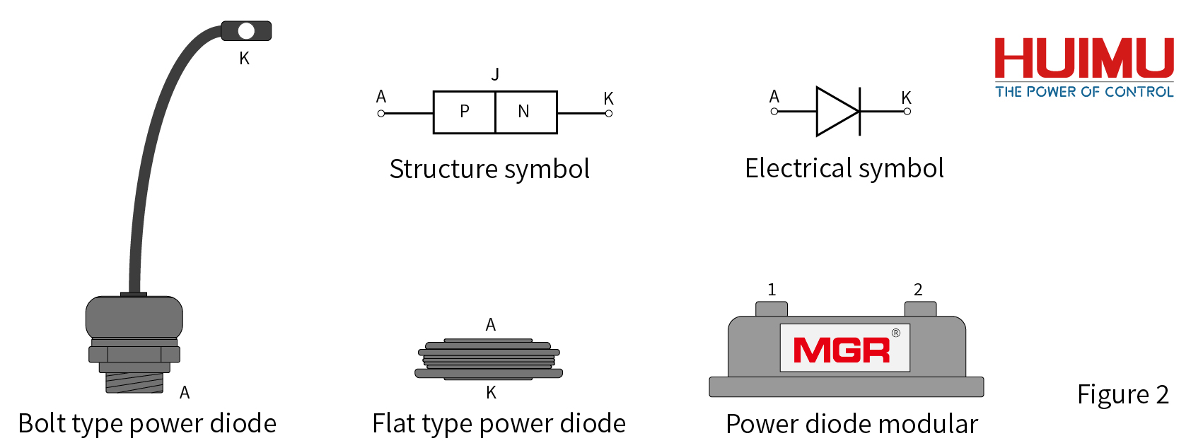
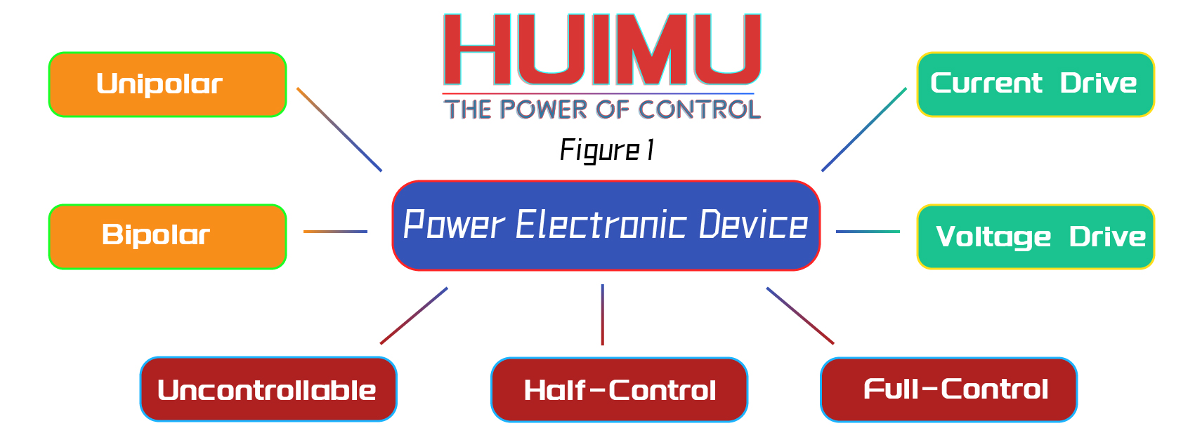
Uncontrollable devices refer to devices that cannot be turned on and off by control signals, so no drive circuit is required. Uncontrollable devices generally refer to power diodes, and their basic structure and working principle are very similar to diodes. The power diode is encapsulated by a large-area PN junction and lead wires at both ends. According to the shape, power diodes can be divided into bolt type and flat type. According to the carriers involved in the conduction process, power diodes can be divided into unipolar power diodes and bipolar power diodes. Power diodes are widely used in power equipment in various fields because of their simple structure and low price. Especially fast recovery diodes and Schottky barrier diodes have an irreplaceable position in the rectification and inverter of low voltage, intermediate frequency and high frequency fields. With the development of modularization and integration technology, modular power diodes are becoming more and more common in the market (click to view more power diode modules).
2.2 How does Power Diode work?
The essence of the power diode is the PN junction formed by the contact between the P-type semiconductor and the N-type semiconductor. Therefore, in order to understand the working principle of the power diode, it is necessary to understand the basic characteristics and working principle of the PN junction.
2.2.1 Basic Structure of PN Junction
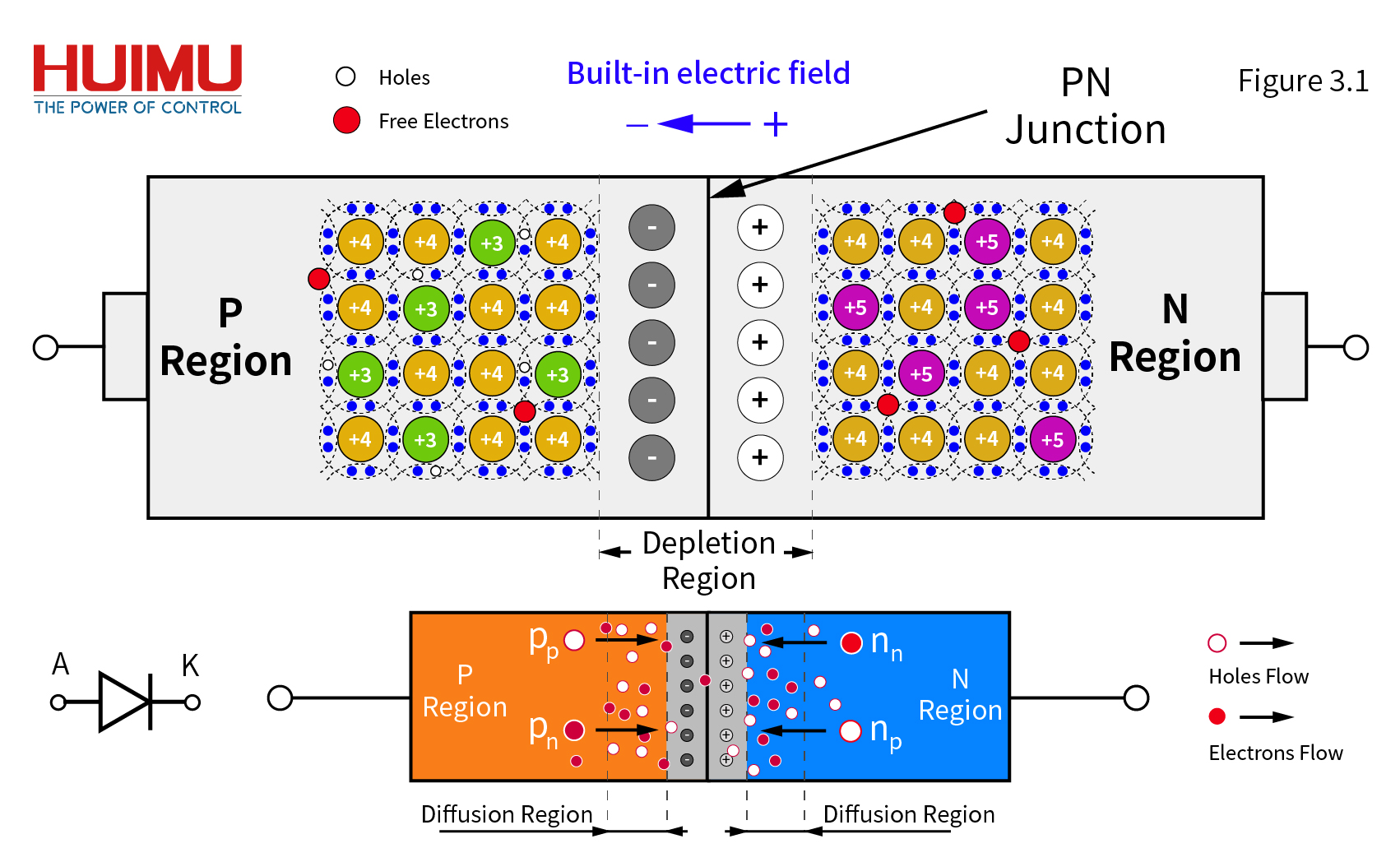
The power diode is composed of a P-type semiconductor and an N-type semiconductor. N-type semiconductors and P-type semiconductors are composed of doped intrinsic semiconductors -- the concentration of free electrons in N-type semiconductors is high; the concentration of holes in P-type semiconductors is high. The connection area between the P-type semiconductor and the N-type semiconductor is called the PN junction. Free electrons and holes are also called free carriers (referred to as carriers) . The movement and recombination of free electrons in the semiconductor will inevitably lead to the generation and recombination of holes. From a macro point of view, this process is more like negatively charged free electrons and positively charged holes moving in opposite directions in the semiconductor at the same time. The movement of free electrons and holes in semiconductors is very fast and random, so it is almost impossible to predict the trajectory of a certain free electron or hole and accurately know its position at a certain moment. However, the movement of a large number of holes and free electrons is not without rules.
Majority carriers in semiconductors will diffuse from high-concentration regions to low-concentration regions -- the majority carrier free electrons (nn) in the N region diffuse from the high-concentration N region through the PN junction to the low-concentration P region; at the same time, the majority carrier holes (pp) in the P region diffuse from the high concentration P region through the PN junction to the low concentration N region. The carriers near the PN junction are depleted due to the diffusion movement, leaving only space charges (positive ions and negative ions) that cannot be moved, so this area is called the space charge region (also known as the depletion region). Since there are no free moving carriers in the space charge area, it is similar to an insulator. The space charge in the space charge region will generate a built-in electric field to prevent carriers from passing through the PN junction (the built-in electric field will be formed within a few nanoseconds after the PN junction is manufactured). Even so, there are still very few carriers that pass through the PN junction and become minority carriers in the opposite region -- free electrons become minority carriers in the P region (pn); holes become minority carriers in the N region (np). This phenomenon is called the quantum tunneling effect. The difference in carrier concentration on both sides of the space charge region produces a built-in potential difference (also called a built-in potential, or contact potential difference). Minority carriers will continue to diffuse into the lower concentration area. The average distance that the minority carriers can reach in the process of diffusion and recombination is called the diffusion length. The diffusion length is affected by the minority carrier lifetime -- the longer the minority carrier lifetime, the longer the diffusion length. When reaching the edge of the diffusion region, the minority carriers will pass through the PN junction and return to their original region under the action of the built-in electric field.
* Single Crystal Semiconductor and Polycrystalline Semiconductor
Single crystal semiconductor refers to a semiconductor with pure chemical composition, no impurities and no lattice defects, that is, intrinsic semiconductor, such as silicon (Si), germanium (Ge), gallium arsenide (GaAs), etc. The structure of single crystal semiconductors is very regular, and its macroscopic properties are anisotropic (in different directions, their physical properties are different). Single crystal semiconductors are the materials for most semiconductor devices.
Polycrystalline semiconductor refers to a semiconductor material composed of a large number of tiny single crystal semiconductor particles with different orientations. The structure of polycrystalline semiconductors does not have regularity, and their macroscopic properties are often isotropic (in different directions, their physical properties are the same). Polycrystalline semiconductors can be used to make narrow-film transistor switch matrices for solar cells, liquid crystal displays, and gate materials for MOSFET.
* Energy Band Theory

Energy band theory is a theory that uses quantum mechanics to study the movement of electrons inside a solid. In a coordinate system with energy as the ordinate, the energy of electrons in the crystal can be represented by a horizontal line -- the greater the energy, the higher the position of the line. Energy levels that are very close to each other within a certain energy range form the energy band. The vertical distance between the highest energy level and the lowest energy level in the energy band is called the energy band width. The position and width of the energy band are affected by the crystal type (such as metal, semiconductor, insulator), temperature and etc. The energy band of a semiconductor is shown in Figure 3.2a.
Full Band: It refers to the energy band that is completely occupied by electrons when T = 0K. The electrons in the full band are valence electrons (that is, electrons that are bound by the valence bonds on the crystal atoms and cannot move freely), so it does not have any conductivity.
Empty Band: It refers to the energy band that is not occupied by electrons when T = 0K. There are no electrons in the empty band, so it does not have any conductivity. The empty band becomes the conduction band when there are electrons in it.
Conduction Band: It refers to the energy band that is not completely occupied by electrons when T > 0K. The electrons in the conduction band are free electrons, so it has conductivity.
Valence Band: It refers to the energy band occupied by valence electrons when T > 0K. The electrons in the valence band are valence electrons, so it does not have any conductivity.
Forbidden Band: It refers to the energy range between the top of the valence band and the bottom of the conduction band. There is no energy level of shared electrons (that is, electrons shared by multiple atoms in the crystal) in the forbidden band, but there are energy levels of non-shared electrons (that is, localized electrons in impurities and defects). The forbidden band width (band gap) reflects the bondage degree of valence electrons or the strength of the valence bond, that is, the minimum average energy required for intrinsic excitation. The middle line of forbidden band is Fermi level.
The band gap of common metal materials is generally very small (the conduction band and the valence band even overlap each other), and their electrons can easily gain energy and transition to the conduction band at room temperature, so their conductivity is strong. The band gap of insulating materials is generally very large (usually greater than 9 electron volts, or 9 eV), and their electrons are difficultly to transition to the conduction band, so their conductivity is very poor. The band gap of semiconductor materials is between conductors and insulators (about 1-3 eV, for example, at room temperature, the band gap of germanium is 0.67 eV, and the band gap of silicon is 1.12 eV), so just give appropriate energy excitation (breaking the valence bond to make the valence electron transition to the conduction band to generate free electrons and holes) or change the band gap (reducing the energy required for electronic transitions) can make the semiconductor conductive.
* Intrinsic Excitation and Free Carriers
Intrinsic excitation means that by giving certain excitation conditions, the electrons in the intrinsic semiconductor will cross the forbidden band from the lower energy band (full band or valence band) into the higher energy band (empty band or conduction band) and becomes the free electrons. It should be noted that the free electrons in the conduction band of the intrinsic semiconductor refer to the approximately free electrons in the solid, which can move freely in the entire solid, but cannot run out of the solid. A positively charged vacancy is formed due to the lack of an electron in the lower energy band, which is called the hole. Free electrons in the conduction band and holes in the valence band are collectively called electron-hole pairs. In intrinsic semiconductors, free electrons and holes generated by intrinsic excitation can move freely, so they are called free carriers, and their concentrations are equal to each other, and as the temperature rises, their concentration will increase exponentially. The directional movement of free electrons and holes will form electrons flow and holes flow. The free electrons in the conduction band will fall into the holes, causing the electron-hole pairs to disappear. This process is called recombination. The energy generated during recombination is released in the form of electromagnetic radiation (emitting photon) or thermal vibration of the lattice (emitting phonon). At a certain temperature, the generation and recombination of electron-hole pairs exist simultaneously and reach a dynamic equilibrium. At this time, the intrinsic semiconductor has a certain carrier concentration and thus it has a certain electrical conductivity. Through intrinsic excitation, more electron-hole pairs are generated, thereby increasing the carrier concentration, which can effectively increase the conductivity of the semiconductor. According to this principle, semiconductor devices such as semiconductor thermistors and semiconductor photo-resistors can be manufactured. The conductivity of intrinsic semiconductors at room temperature is small, and the carrier concentration is sensitive to temperature changes, so it is difficult to effectively control the semiconductor characteristics of their semiconductors through temperature.
Intrinsic excitation methods can generally be divided into intrinsic thermal excitation, intrinsic light excitation, and impact ionization intrinsic excitation.
Intrinsic Thermal Excitation: It refers to the infrared photons radiated by thermal motion of molecules as the temperature increases, which makes valence electrons to gain enough energy to break free from the bondage of valence bonds and become free electrons. The energy required for intrinsic thermal excitation is equal to the band gap. The thermal excitation efficiency at room temperature is usually very limited, because a very high temperature is required to allow enough carriers to transition to the conduction band.
Intrinsic Light Excitation: It refers to the photons radiated by light (generally referring to visible light or ultraviolet light), which makes valence electrons to gain enough energy to break free from the bondage of valence bonds and become free electrons. The energy required for intrinsic light excitation is greater than intrinsic thermal excitation. Since the photons of visible light have higher energy than the infrared photons usually generated by thermal motion, the energy of electrons after intrinsic light excitation is usually located at a higher position in the conduction band. Because the momentum of the photon can be ignored, the intrinsic light excitation does not change the momentum of the electron, so this process is also called the vertical transition. But if there is a phonon (referring to the simple harmonic vibration of the crystal lattice) involved, the momentum of the electron will change, so it is also called a non-vertical transition.
Impact Ionization Intrinsic Excitation: It refers to the collision and ionization of valence electrons by high-energy electrons (that is, free electrons accelerated by an electric field) to become free electrons. The average energy required for impact ionization intrinsic excitation is about 1.5 times the band gap. The electrons produced by the intrinsic excitation of impact ionization are ionized electrons, which are the truly free electrons that can leave the solid, and their energy exceeds the free electrons with the highest energy level in the conduction band.
* Fermi Level and Fermi-Dirac Distribution
The Fermi level is the energy level that has a 50% chance of being occupied by electrons at any temperature -- below the Fermi level, the farther the distance is, the greater the possibility of being occupied by the electrons; above the Fermi level, the farther the distance is, the less the possibility of being occupied by the electrons. For semiconductors, especially intrinsic semiconductors, the Fermi level is in the middle line of the forbidden band. When the temperature T = 0K, the full band is filled with electrons (the electron occupancy probability is 1), and the empty band has no electrons at all (the electron occupancy probability is 0), then their Fermi level is exactly at the middle line of the forbidden band (the electron occupancy probability is 1/2). Even when the temperature rises T> 0K, intrinsic excitation will produce electron-hole pairs, but since the number of electrons increased in the conduction band is equal to the number of electrons decreased in the valence band, the Fermi level is still in the middle line of the forbidden band (the electron occupancy probability is 1/2). Therefore, the position of the Fermi level of the intrinsic semiconductor does not change with temperature and is always at the middle line of the forbidden band. The Fermi-Dirac distribution of electrons can be calculated from the Fermi level and temperature, as shown in Figure 3.2b.
* Semiconductor Doping
Generally, intrinsic semiconductor will be doped to introduce new energy levels to increase its conductivity. The doped semiconductor is more susceptible to external influences (such as light, temperature rise, etc.).
By doping the silicon crystal (or germanium crystal) with phosphorus element (or antimony element), the phosphorus atom (or antimony atom) will occupy the position of the silicon atom. Then a set of full energy levels will be added to the position in the forbidden band which is very close to the conduction band. The electrons on these energy levels can easily transition to the conduction band to become free electrons. Therefore, the phosphorus element (or antimony element) is called a donor impurity (or N-type impurity), and a semiconductor doped with an N-type impurity is called an N-type semiconductor.
By doping the silicon crystal (or germanium crystal) with boron element (or indium element), the boron atom (or indium atom) will occupy the position of the silicon atom. Then a set of empty energy levels will be added to the position in the forbidden band which is very close to the valence band. The electrons in the valence band can easily transition to these energy levels and leave holes in the valence band. Therefore, boron element (or indium element) is called acceptor impurities (or P-type impurities), and semiconductors doped with P-type impurities are called P-type semiconductors.
2.2.2 Unidirectional Conductivity of PN Junction
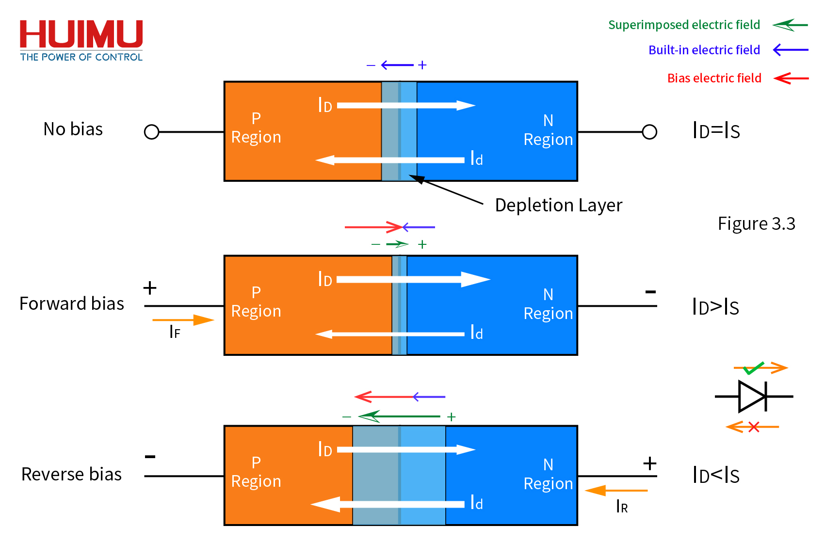
The essence of the working principle of the power diode is the unidirectional conductivity of the PN junction. In the case of constant external conditions (temperature, radiation, etc.), the external circuit will supplement the carriers consumed during the operation of the power diode, so the conductivity of the power diode is mainly affected by its internal carrier concentration.
Forward Conduction State: If a forward bias voltage is applied across the power diode, the majority carriers will move closer to the PN junction, which will narrow the space charge region and weaken the built-in electric field, but the PN junction will still maintain dynamic equilibrium state. Only when the forward bias voltage is greater than the built-in electric field, the dynamic equilibrium can be broken, and a superimposed electric field in the opposite direction of the drift current is generated. The diffusion current ID is greater than the drift current Id. The current flowing through the PN junction is the forward current IF. Due to the built-in potential difference, when the power diode is in the forward conducting state, an on-state voltage drop will be generated at both ends of it, which makes the power diode present a low impedance state. The on-state voltage drop of the power diode is not a fixed value, it is proportional to the current flowing.
Reverse Cut-off State: If a reverse bias voltage is applied across the power diode, the majority carriers will move away from the PN junction, which will widen the space charge region and enhance the built-in electric field. The dynamic equilibrium of the PN junction is broken, and a superimposed electric field in the same direction as the drift current is generated. The drift current Id is greater than the diffusion current ID. The current flowing through the PN junction is the reverse saturation current Isat. Because the number of minority carriers is too small, the reverse saturation current of the power diode is usually negligible, which makes the power diode present a high impedance state.
Reverse Breakdown State: If the reverse bias voltage across the power diode continues to increase to a certain critical value, the number of carriers in the power diode increases rapidly, causing the reverse current IR to increase significantly. In the reverse breakdown state, the power diode presents a no-impedance state, and its reverse current IR and reverse voltage UR are both very large. The reverse breakdown of PN junction is mainly divided into avalanche breakdown and Zener breakdown. Both of these breakdowns will increase the temperature of the PN junction, and eventually lead to thermal breakdown, which will cause permanent damage to the PN junction. If the cooling measures are done well enough, even if the power diode is reverse broken down, but the PN junction is not destroyed, then after limiting or closing the reverse voltage, the PN junction can still be restored to its original state.
* Diffusion Current and Drift Current
Diffusion motion refers to the movement of majority carriers from a high-concentration area to a low-concentration area. The diffusion motion is determined by the concentration gradient. Drift motion refers to the movement of minority carriers returning to the original area under the action of the built-in electric field. The drift motion is determined by the built-in electric field. Diffusion motion and drift motion are the basic motions of carriers in the PN junction. The current generated by the diffusion motion is called the diffusion current ID, and the current generated by the drift motion is called the drift current Id. When there is no applied voltage (or the forward bias voltage is less than the built-in electric field), the diffusion motion will cause the built-in electric field to enhance and the drift current will increase; the drift motion will cause the built-in electric field to weaken and the diffusion current to increase. Finally, the diffusion current is equal to the drift current, and the PN junction will be in a dynamic equilibrium state where the total current is zero.
* Avalanche Breakdown and Zener Breakdown
Avalanche breakdown usually occurs in a low-doped PN junction with a wide depletion layer. Due to the wide depletion layer, when the reverse bias is large, the free electrons in the semiconductor will continuously accelerate under the electric field force, and obtain a large number of kinetic energies. These high-energy electrons collide with valence electrons, freeing them from the bondage of valence bonds and generating new electron-hole pairs. These newly generated free electrons continue to repeat this process under the action of the electric field force, causing the free carriers in the semiconductor to increase rapidly like an avalanche, leading to a sharp increase in drift current. The essence of the avalanche breakdown is the impact ionization excitation, so the avalanche breakdown voltage is usually high (generally higher than 6V). The avalanche breakdown voltage increases with the increase of temperature, mainly because the irregular thermal movement of carriers increases with the increase of temperature, so a larger reverse voltage is required to provide a large enough electric field to make the carriers do directional acceleration motion.
Zener breakdown usually occurs in a highly doped PN junction with a narrow depletion layer. Due to the narrow depletion layer, there is not enough space for free electrons to accelerate, so avalanche breakdown will not occur. At the same time, due to the narrow depletion layer, even if the reverse bias is not large, a strong electric field can still be generated in the PN junction, pulling electrons out of the valence bond, and generating new electron-hole pairs. This phenomenon is also called field-induced excitation. Field-induced excitation will greatly increase the number of carriers in the semiconductor, thereby significantly increasing the drift current. Zener breakdown voltage is usually low (generally less than 4V). The Zener breakdown voltage decreases with increasing temperature, mainly because the electrons in the valence bond become more active with increasing temperature, so it is more easily for the electric field force to pull them out.
2.2.3 Capacitance Effect of PN Junction
The amount of charge in the PN junction changes with the applied voltage, exhibiting a capacitance effect. This capacitance is called the junction capacitance CJ (also known as differential capacitance). According to the different generation mechanism and function, the junction capacitance CJ can be divided into the barrier capacitance CB and the diffusion capacitance CD, and they conform to the calculation formula CJ=CB+CD. Both the barrier capacitance and the diffusion capacitance are non-linear capacitance.
1- Barrier Capacitance
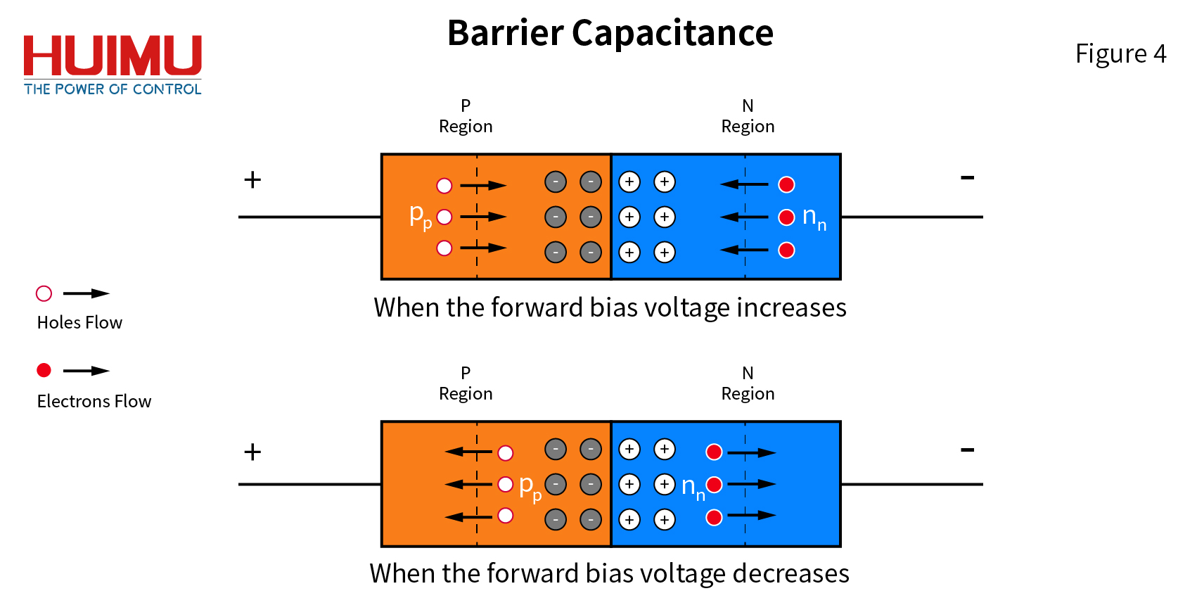
The narrow layer of ions in the space charge region (depletion layer) forms the barrier region. The number of space charges in the barrier area changes with the applied bias voltage, which is equivalent to the charge and discharge effect of the capacitor -- when the forward bias voltage increases, the barrier area decreases, which is equivalent to storing free electrons or holes into the barrier area; when the forward bias decreases, the barrier area increases, which is equivalent to taking out free electrons or holes from the barrier area. The equivalent capacitance of the barrier region is called the barrier capacitance CB. If the frequency of the applied bias voltage is higher, the effect of the barrier capacitance is more obvious. Regardless of low-frequency operation or high-frequency operation, the barrier capacitance may deteriorate the unidirectional conductivity of the semiconductor device, or even fail to work. In fact, the maximum operating frequency of a semiconductor device is often determined by the barrier capacitance. It is worth noting that the barrier capacitance is the capacitance effect related to the majority carrier (pp and nn), and neither the forward bias nor the reverse bias can be ignored. In forward bias, when the forward voltage is low, the barrier capacitance is much larger than the diffusion capacitance, so the barrier capacitance is the main component of the junction capacitance, CJ ≈ CB.
2- Diffusion Capacitance
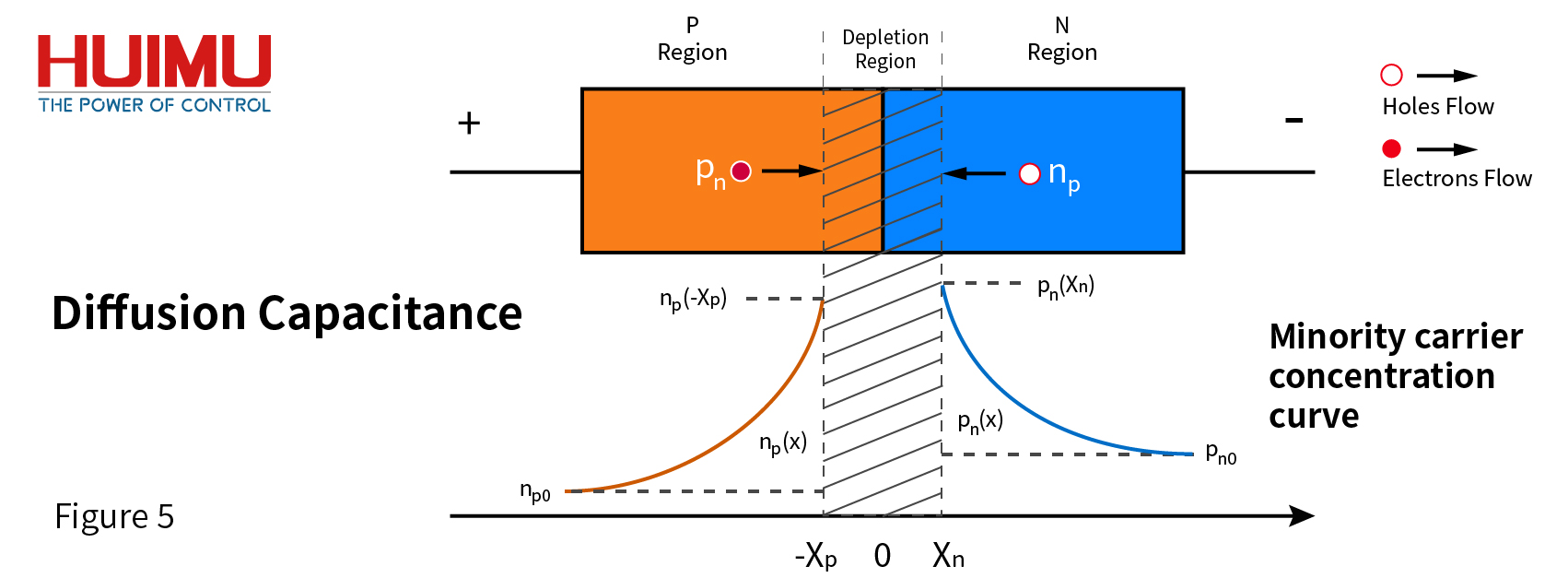
When the PN junction is forward biased, the built-in electric field is weakened, and the drift motion of minority carriers is weakened. The diffusion current is greater than the drift current. Therefore, the carriers that diffuse to the opposite area will accumulate at the barrier boundary to form a certain concentration of non-equilibrium minority carriers (pn and np) -- the closer to the PN junction, the higher the concentration; the farther away from the PN junction, the lower the concentration. The amount of charge of such non-equilibrium minority carriers changes with the forward bias, which is equivalent to the charge and discharge effect of the capacitor -- when the forward bias increases, the non-equilibrium minority carriers are increased, which is equivalent to the charging of the capacitor; when the forward bias decreases, the non-equilibrium minority carriers are reduced, which is equivalent to the discharging of the capacitor. The equivalent capacitance at the boundary of the barrier region is called the diffusion capacitance CD. The diffusion capacitance has a great influence on the switching speed of the PN junction when working at low frequencies, and can be ignored when working at high frequencies. In forward bias, if the forward voltage is high, the diffusion capacitance is much larger than the barrier capacitance, so the diffusion capacitance is the main component of the junction capacitance, CJ ≈ CD. In reverse bias, there are too few non-equilibrium minority carriers, and the diffusion capacitance can be ignored, so the barrier capacitance is the main component of the junction capacitance, CJ ≈ CB.
2.3 Main Parameters of Power Diodes
1- Maximum Forward Average Current IFM(AV)
The maximum forward average current IF(AV) is the rated current of the power diode, which refers to the average value of the maximum power frequency half-wave sine current allowed to flow through the power diode under the specified case temperature TC and heat dissipation conditions. If it exceeds IF(AV), the diode will be burned out. Since the waveform of some power diodes is not necessarily a half-sine wave, and some power diodes do not have resistance characteristics, IF(AV) is defined according to the thermal effect of current, that is, find a resistor with similar heat generation according to the principle of equal effective value. Considering that the heat dissipation conditions will affect the ability of the power diode to withstand current, it is recommended to leave a certain margin to avoid damage to the power diode due to heat dissipation problems.
2- Threshold Voltage UTO
The threshold voltage UTO (also known as the dead zone voltage) is the lowest forward voltage at which the power diode can be turned on. The threshold voltage is the lowest forward voltage drop of the power diode. The threshold voltage of germanium crystal is about 0.1V; the threshold voltage of silicon crystal is about 0.5V.
3- On-state Voltage Drop UCO
The on-state voltage drop UCO (also known as the conduction voltage) is the forward voltage drop when the power diode is turned on and works stably. Ideally, the on-state voltage drop of the power diode is equal to the built-in potential. The built-in potential is related to the degree of semiconductor doping and is approximately equal to the half of the band gap. The on-state voltage drop of the power diode is proportional to the current flowing. The on-state voltage drop of germanium crystals is usually around 0.1-0.3V; the on-state voltage drop of silicon crystals is usually around 0.5-0.8V.
4- Maximum Forward Voltage Drop UFM
The maximum forward voltage drop UFM is the forward voltage drop corresponding to the maximum forward average current IFM(AV) at a specified temperature.
5- Reverse Saturation Current Isat
When an appropriate reverse voltage is applied, a very small leakage current will be generated, which is called the reverse saturation current Isat. The reverse saturation current is generated by the drift motion of minority carriers, so it is greatly affected by temperature.
6- Reverse Repetitive Peak voltage URRM
The reverse repetitive peak voltage URRM (also known as the maximum reverse voltage URM) is the rated voltage of the power diode, which refers to the highest reverse voltage that the power diode can withstand repeatedly applied. If it exceeds this value, the power diode will be reversed and damaged. Taking into account the overvoltage in the circuit and other factors, when using power diodes, there should usually be a double margin. For example, a power diode with a rated voltage of 1000V can only be used as a 500V power diode.
7- Reverse Recovery Time trr
The reverse recovery process is caused by the capacitance effect of the power diode. When the switch transitions from the on state to the off state, the power diode needs to release the charge stored in the junction capacitance before blocking the reverse current. This discharge time is called the reverse recovery time trr, that is, the time from when the forward conduction current is zero to when it enters the fully turn-off state. The reverse recovery time of power diodes of different specifications is different, so you need to fully consider when designing the circuit, otherwise it may cause unnecessary trouble. For example, the reverse recovery time of a power diode is Trr. If a continuous PWM wave with a period of T1 (T1<Trr) passes through the power diode, the PWM wave cannot be blocked when the power diode is reversely biasing.
8- Maximum Operating Junction Temperature TJM
The junction temperature TJ refers to the average temperature of the PN junction. The maximum operating junction temperature TJM refers to the highest average temperature that the PN junction can withstand without damage (usually the highest junction temperature of germanium transistors is about 75°C, and the highest junction temperature of silicon transistors is about 150°C). Temperature has a very significant impact on the working characteristics of power diodes, so sufficient heat dissipation conditions must be provided to avoid damage to the power diode due to overheating.
9- Maximum Operating Frequency fM
The maximum operating frequency fM is the upper turn-off frequency of the diode. If the frequency is too high, the power diode will easily lose its ability to block reverse current due to the capacitive effect. At the same time, if the frequency is too high, it will also cause the power diode to be burned due to the increase of on-state power consumption.
10- Surge Current IFSM
The surge current IFSM refers to the maximum continuous overcurrent of one or several power-frequency cycles that the power diode can withstand.
2.4 Basic Characteristics of Power Diodes
2.4.1 Static Characteristics of Power Diodes
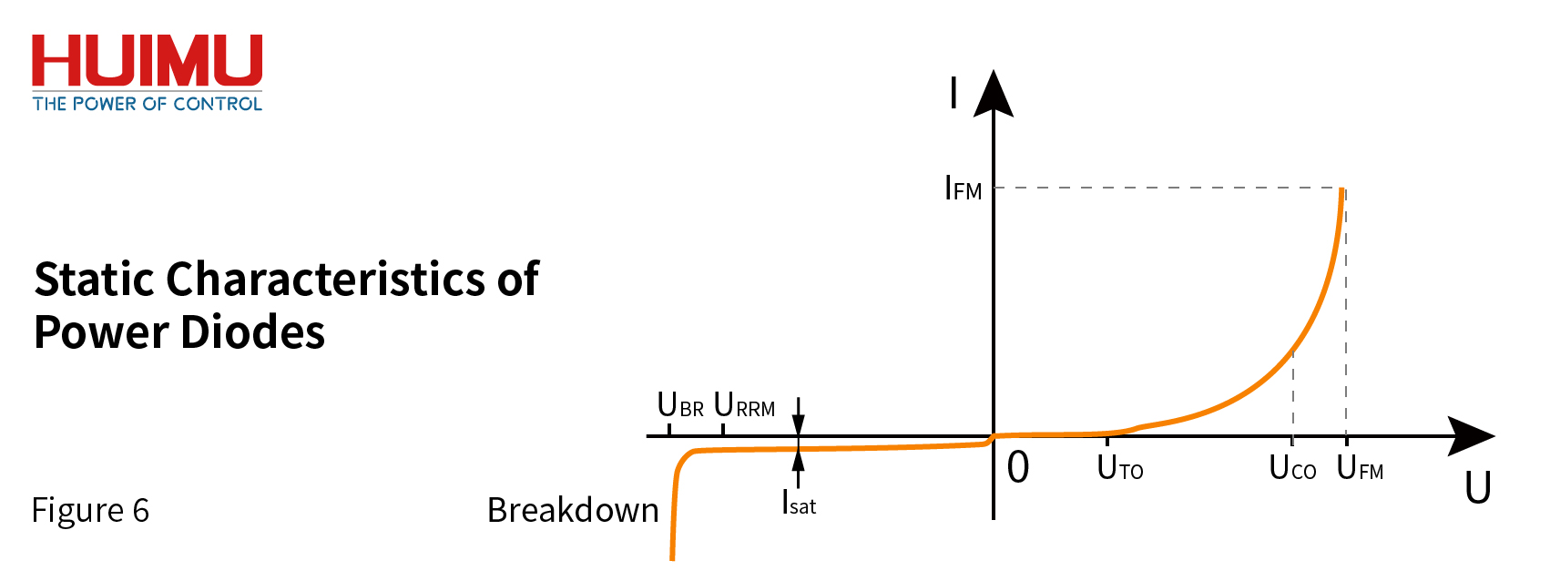
The static characteristic of the power diode mainly refers to the volt-ampere characteristic curve of the power diode, shown in Figure 6.
When a forward bias voltage is applied to both ends of the power diode, the power diode will not be turned on immediately. Only when the forward voltage is greater than the threshold voltage UTO of the power diode, the power diode will be turned on. At this time, the forward current IF begins to increase significantly, until the power diode is in a stable conduction state, at which time the diode's conduction voltage is UCO. If the forward current reaches IFM, the corresponding voltage drop is UFM, and the power diode will be burned out due to excessive current.
When a reverse bias voltage is applied to both ends of the power diode, the power diode will not conduct, but will generate a small constant value current, that is, reverse leakage current. When the reverse voltage reaches the reverse UBR of the power diode, the power diode will be reversely broken down, and the reverse current will become very large at this time.
2.4.2 Dynamic Characteristics of Power Diodes
The dynamic characteristics of the power diode refer to its switching characteristics, that is, the voltage-current characteristic of the power diode during the transition between on-state and off-state. Because of the junction capacitance, the voltage-current characteristics of power diodes change with time.
1- Turn-on process
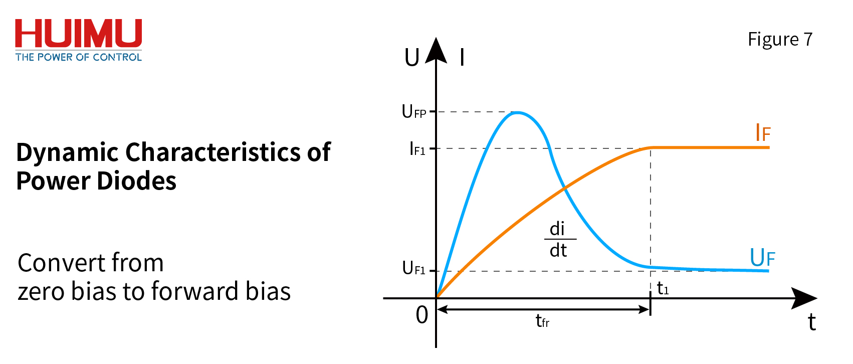
The dynamic characteristic of the power diode in the turn-on process is shown in Figure 7. When the voltage changes from zero bias to forward bias, the forward current IF of the power diode will increase from 0 to IF1. Due to the large di/dt, under the action of the line inductance, a forward peak voltage UFP will be generated at both ends of the power diode. After a certain period of time, the forward voltage UF will gradually drop from UFP to the stable voltage UF1 (that is, the on-state voltage drop). In this process, the time when the forward current rises from 0 to IF1 is called the forward recovery time tfr.
2- Turn-off process
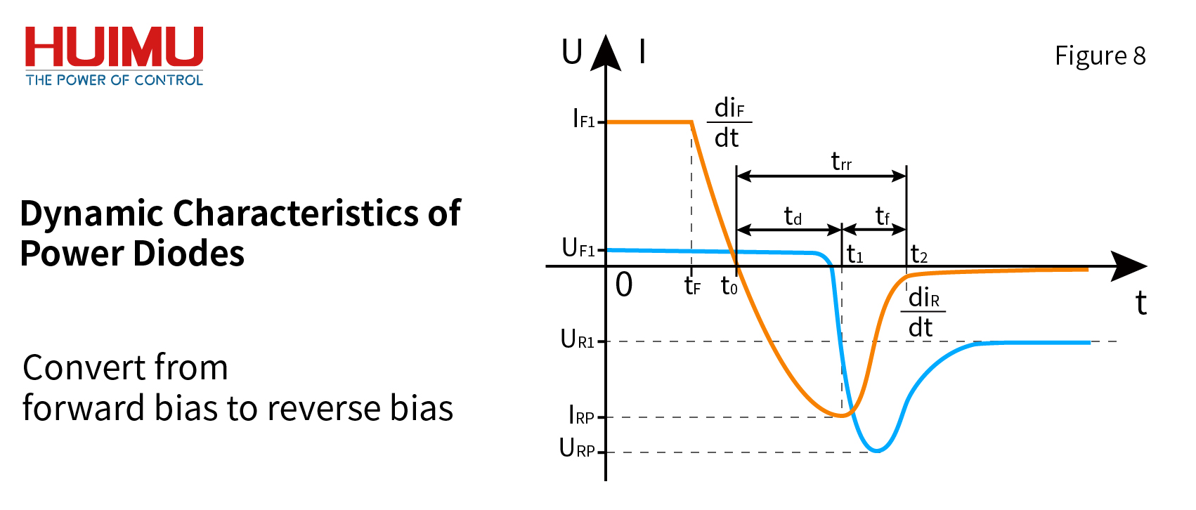
The dynamic characteristic of the power diode in the turn-off process is shown in Figure 8. Due to the junction capacitance, even if the forward bias is converted to the reverse bias, the power diode will not be turned off immediately, but it will take a period of time to regain the reverse blocking capability.
When the power diode is switched from forward bias to reverse bias at tF, and the forward current IF decreases rapidly, and drops to 0 at t0, and diF/dt is large. From t0 to t1, the current not only does not disappear, but becomes the reverse current IR and increases rapidly until it reaches the maximum value IRP. This time period is called the delay time td. From t1 to t2, the reverse current begins to drop sharply to a very small value. This time period is called the fall time tf. From t2, the reverse current begins to slowly decrease until it drops to 0 (in fact, there is still a very small reverse leakage current). The time from t0 to t2 is called the reverse recovery time trr, during which the power diode is reverse conducting. The reverse recovery time trr determines the operating frequency of the power diode. If the operating frequency of the external circuit is too high, the power diode cannot enter the reverse cut-off state when reverse biased, and there is a large reverse current, which is equivalent to the power diode losing its reverse blocking ability.
Before the reverse current rises to the maximum value, the voltage across the power diode drops rapidly from the on-state voltage drop UF1 to 0. At the same time, since tf is usually very short, diR/dt is very large. Under the action of the line inductance, a reverse peak voltage URP is quickly generated at both ends of the power diode, and then it begins to drop to a stable value UR1. The reverse peak voltage is usually very large and may break down the power diode. Therefore, increasing the proportion of tf in trr will help reduce the reverse peak voltage. The recovery coefficient (Sr=tf/td) is usually used to express the softness of the reverse recovery characteristics of the power diode.
2.5 Main Types of Power Diodes
1- General Purpose Diode
General purpose diodes (GPD), also known as rectifier diodes, have a long recovery time, high forward current rating and reverse voltage rating. They are mostly used in rectifier circuits with low switching frequency (below 1kHz), and generally cannot be used in medium and high frequency circuits.
2- Fast Recovery Diode
The internal structure of the fast recovery diode (FRD) is different from that of the general purpose diode. It adds a base area I between the P-type and N-type silicon materials to form a P-I-N structure. Because the base area is very thin and the reverse recovery charge is small, it not only greatly reduces trr and the transient forward voltage drop, but also improves its reverse voltage withstand capability. The recovery time of the fast recovery diode is very short (trr>100ns, usually several hundred ns), its forward voltage drop is about 0.6V, the forward current is several amperes to several thousand amperes, and the reverse peak voltage can reach several hundred to several thousand volts. Ultra-fast recovery diodes, also known as fast recovery epitaxial diodes (FRED), have a further reduced reverse recovery charge, so they have a shorter recovery time (trr<100ns, as low as 20~30ns). The forward voltage drop of ultra-fast recovery diodes is also very low (about 0.9V), but its reverse withstand voltage capability is usually not high (less than 1200V).
3- Schottky Barrier Diode
Schottky Barrier Diode (SBD) is a kind of power diode based on the barrier formed by the contact between metal and semiconductor. Compared with general purpose diodes and fast recovery diodes, Schottky barrier diodes have the advantages of short reverse recovery time, no obvious forward voltage overshoot, and high reverse withstand voltage, but their reverse leakage current is large. The forward voltage drop of a Schottky barrier diodes is affected by the reverse withstand voltage -- if the reverse withstand voltage increases, the forward voltage drop will increase significantly. But when the reverse withstand voltage is low, the forward voltage drop of Schottky barrier diodes is significantly lower than that of general purpose diodes and fast recovery diodes, so the switching loss and on-state loss are very low. Therefore, Schottky barrier diodes are usually used in rectifier circuits below 200V. However, it should be noted that Schottky barrier diodes are very sensitive to temperature, so their operating temperature must be strictly limited.


 Introduction:
 Introduction:
 Introduction:
 Introduction:
 Introduction:
 Introduction:
 Introduction:
 Introduction:
 Introduction:
 Introduction:
 Introduction:
 Introduction:
 Introduction:
 Introduction:
 Introduction:
 Introduction:
 Introduction:
 Introduction: