5.1 Introduction to Fully-controlled Devices
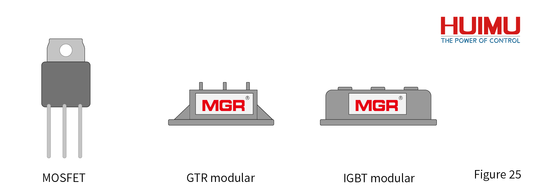
The fully-controlled device (also called the self-shut-off device) is a device that can be controlled by a control signal to be turned on and to be turned off. Since the birth of fully-control devices in the 1980s, power electronics technology has entered a new era. There are many types of fully-controlled devices, most of which use composite structures, each with its own characteristics, which can meet the needs of various fields. Fully-controlled devices mainly include gate-off thyristors (GTO), bipolar junction transistors (including GTR, etc.), field effect transistors EFT (including MOSFET, JFET, etc.), and composite devices (including IGBT, MCT, SIT, SITH, IGCT, etc.). The following content will give a brief introduction to them.
5.2 Gate Turn-off Thyristor
5.2.1 Introduction to GTO
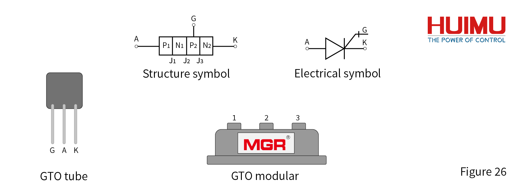
The gate turn-off thyristor (GTO) is a derived device of the thyristor, which appeared soon after the advent of the thyristor. The ordinary thyristor (SCR) is the half-controlled device, and the gate signal no longer has any effect after the SCR is turned on. The GTO is the fully-controlled device that can be turned off by applying a negative pulse signal to the gate.
5.2.2 How does the GTO work?
5.2.2.1 Basic Structure of GTO
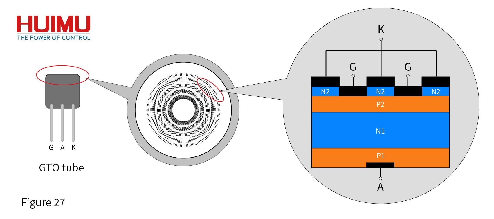
Although the structure of GTO is similar as the SCR, GTO has one more N+ buffer region, so the turn-on time of GTO is shorter than SCR, but at the same time its reverse blocking ability is weaker than SCR. GTO is a multi-unit power integrated device, which is composed of dozens or even hundreds of GTO units with a common anode. The cathodes and gates of these GTO units are connected in parallel inside the device. The cathode region of each GTO unit in this integrated structure is small, and the distance between the gate and the cathode is greatly shortened, which makes the P2 base region small in lateral resistance and can draw a larger current from the gate, which makes the collector of V1 is easy to be cut off, and finally makes the thyristor easy to be turned off. This integrated structure also makes the turn-on speed of GTO faster than that of SCR, and has stronger di/dt bearing capacity and overload bearing capacity -- SCR has only one unit, once the di/dt is too large, it is easy to be damaged by local overload and overheating; any local area of GTO is composed of multiple small GTO units, and the overload and overheating caused by the di/dt will be dispersed to these small GTO units. The volume of GTO is much smaller than SCR, so its capacity density is higher than SCR. At the same time, GTO does not require a commutation circuit, so it can be used in applications above 1kHz, while SCR can only be used in applications within 1kHz. But the reverse blocking ability of GTO is weaker than SCR, usually 20-30V. Because of these advantages, GTO is widely used in high-power applications above the megawatt level.
Generally, a power diode will be connected in anti-parallel to GTO to optimize its switching characteristics. In order to facilitate design and use, the power diode is normally integrated in GTO to form a reverse-conducting GTO, which is a bit similar to a reverse-conducting thyristor. The reverse-conducting GTO no longer has the ability to withstand reverse voltage. If it needs to withstand the reverse voltage, a power diode is required in series.
5.2.2.2 Working Principle of GTO
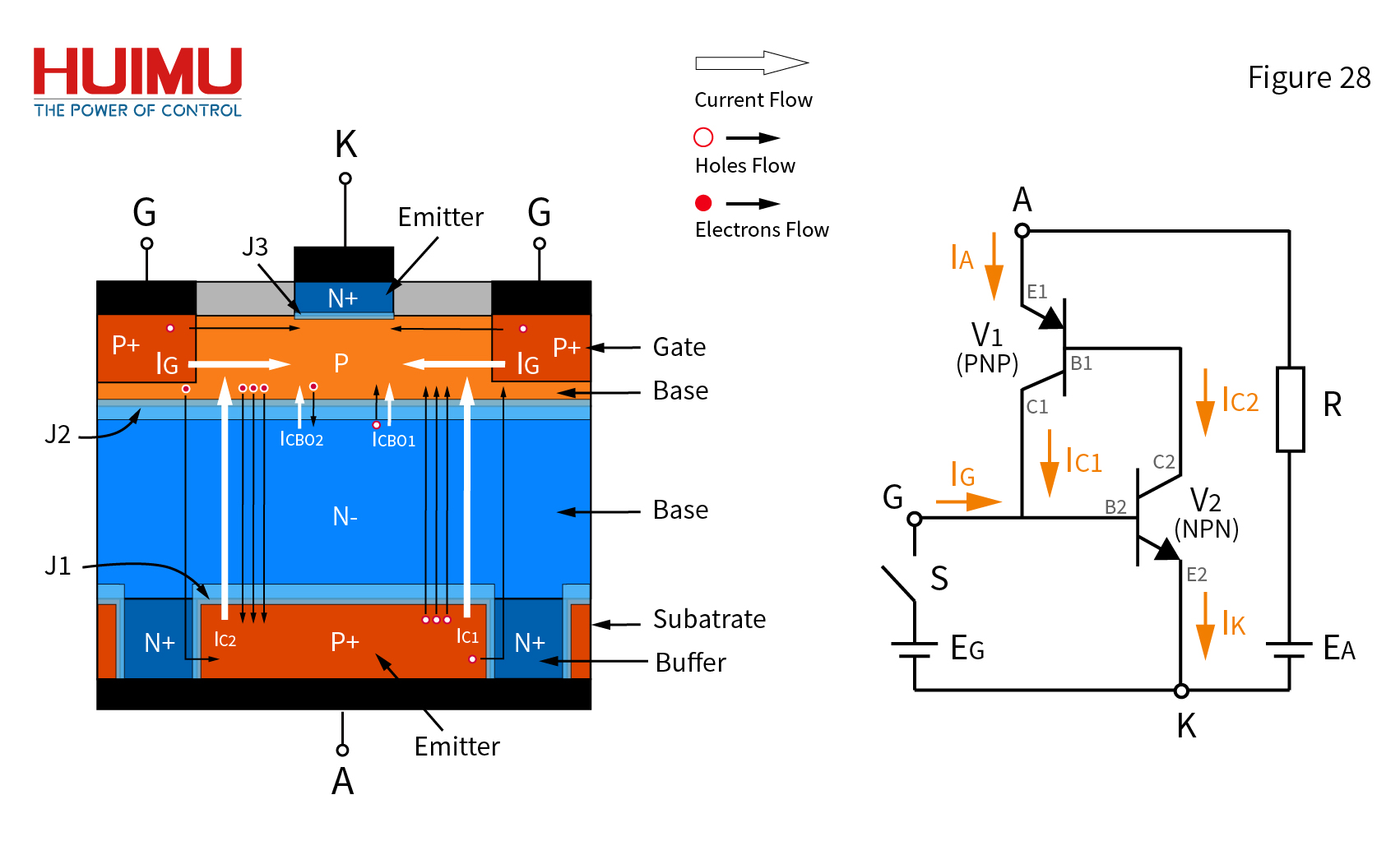
The turn-on principle of GTO is similar to the turn-on principle of thyristor. The N+ region contributes to the reduction of conductivity to speed up the positive feedback process. The α1 of GTO is designed to be small, which makes the saturation depth of GTO shallower than SCR, so it is easier to be cut off -- when SCR is on, α1 + α2 ≥ 1.15; when GTO is on, α1 + α2 ≈ 1.05, which is close to critical saturation. This design makes the equivalent transistor V2 more sensitive to the gate control signal, which makes V2 easy to be turned on and turned off, but at the same time, it also makes the on-state voltage drop of GTO increases. During the turn-off process, a sufficiently large negative current is passed into the gate to consume holes in the P base region and inject a large number of free electrons into the N- base region, with the holes of the P+ region injected into the base region decrease, IC1 gradually decreases, and IC2 also decreases. After a series of positive feedback process, when the anode current IA is less than the holding current IH, the GTO is cut off due to exiting saturation.
The calculation formula of GTO is the same as the calculation formula of thyristor.
IC1 = α1 * IA + ICBO1, (10)
IC2 = α2 * IK + ICBO2, (11)
IK = IA + IG, (12)
IA = IC1 + IC2, (13)
IA = (α2 * IG + ICBO1 + ICBO2) /[1 - (α1 + α2) ]. (14)
|IGRP|>(α1 + α2-1) * IATO/α2, (15)
βoff=IATO/|IGRP|. (16)
It can be seen from Formula 14:
When α1+α2 approaches 0, IA will tend to leak current;
When α1+α2 approaches 1, IA will tend to infinity.
5.2.3 Main Parameters of GTO
Most of the parameters of GTO are the same as the main parameters of SCR.
1- Turn-on time ton
The turn-on time ton is the sum of the delay time td and the rise time tr.
2- Turn-off time toff
The turn-off time toff is the sum of the storage time ts and the fall time tf.
3- Maximum Controllable Anode Current IATO
The maximum controllable anode current IATO is the rated current of GTO. If the anode current IA is greater than IATO, α1 + α2 cannot meet the condition slightly greater than 1, which will deepen the saturation so that GTO cannot be turned off normally.
4- Current Turn-off Gain βoff
The current turn-off gain βoff is the ratio of the maximum controllable anode current IATO to the peak gate negative pulse current IGRP. βoff=IATO/IGRP. Because the βoff of GTO is too small (usually 3-8), GTO can only be cut off by applying a very large negative current to the gate, which is equivalent to using a strong current to control a strong current. For example, a GTO with a rated current of 1000A requires a gate turn-off current of 300A. This main disadvantage limits the application of GTO.
5.2.4 Basic Characteristics of GTO
5.2.4.1 Static Characteristics of GTO
The static characteristics of GTO are the same as the static characteristics of SCR, but the latching current IL (2A) of GTO is larger than that of SCR (100-500mA).
5.2.4.2 Dynamic Characteristics of GTO
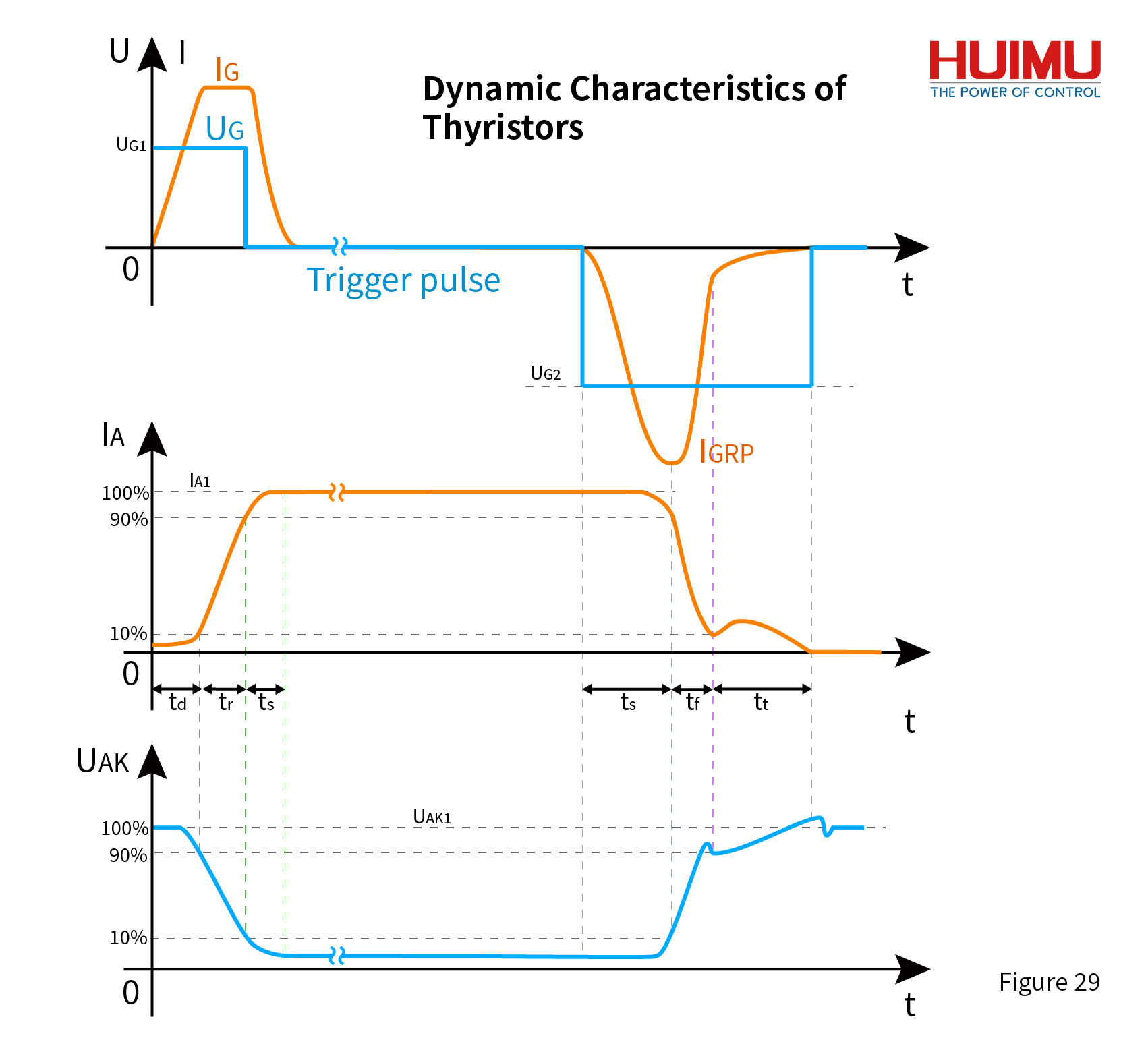
1- Turn-on Process
Similar to the turn-on process of SCR, when UAK=100% UAK1, and UG ≥ UGT, GTO will enter the conducting state, and its output terminal will generate a small on-state voltage drop. However, due to the multi-unit structure of GTO, its gate trigger current IGT is higher than that of SCR. The delay time td of GTO is about 1-2μs. The rise time tr of GTO increases with the increase of the on-state anode current.
2- Turn-off Process
Different with SCR, when a negative pulse voltage is applied to the gate to provide a large enough negative pulse current, GTO enters the turn-off process. The turn-off process of GTO is divided into the storage time ts, the fall time tf, and the tail time tt.
The storage time ts is the time required for IA to decrease from 100% IA1 to 90% IA1. When the turn-off signal UG2 is applied, the negative gate current rises rapidly from 0 to IGRP. The di/dt of the negative gate current depends on the circuit inductance and anode voltage. The negative gate current extracts the carriers stored during saturated conduction from the P base region of the GTO, so that the equivalent transistor V2 exits saturation. Within this period, GTO has not completely exited saturation, so UAK and IA remain unchanged.
The fall time tf is the time required for IA to decrease from 90% IA1 to 10% IA1. When the negative pulse current reaches IGRP, the anode current IA starts to drop rapidly, and the anode voltage UAK starts to rise. As the conductivity of the base region decreases, α1 + α2≤1, GTO begins to enter the turn-off state. Since the fall time tf is very short (about 2μs), and the fall rate of IA is very large, there will be a spike voltage at the output terminal of GTO.
The tail time tt is the time required for IA to decrease from 10% IA1 to 0. During this period, the remaining carriers will recombine, UAK gradually rises to UAK1, and IA gradually decreases to 0. Due to the snubber circuit, there will be a transient overshoot at the output terminal of GTO. If the voltage rise rate of UAK is too large, GTO may turn on again. By maintaining a proper gate negative pulse, the tail time tt can be effectively shortened.
Normally, the fall time tf is less than the storage time ts, and the storage time ts is less than the tail time tt, that is, tf <ts <tt. When IA drops to 10% IA1, it can be considered that GTO has been cut off, so the calculation formula for the turn-off time is: toff = ts + tf.
5.3 Giant Transistor
5.3.1 Introduction to GTR
The giant transistor (GTR) was born in the 1970s, which is a kind of bipolar junction transistor that can withstand high voltage and high current, so GTR is also known as the power BJT. The switching time of GTR is much shorter than that of thyristor and GTO (usually a few microseconds), so GTR has a higher operating frequency -- the operating frequency of thyristor is generally tens of Hz; the operating frequency of GTO is generally several hundred Hz; the working frequency of GTR is generally 1-20kHz. The power capacity of GTR is very large, such as 1800V/800A/2kHz, 1400v/600A/5kHz, and 600V/3A/100kHz. Since GTR has the advantages of low saturation voltage, good switching characteristics, wide safe operating area, large power capacity, and strong self-shut-off capability and etc., so GTR replaces the place of thyristors, and is widely used in medium-capacity and medium-frequency fields, such as power supplies, motor control, and general inverters. However, the drive power required by the GTR is large, and the design of its drive circuit is very complex. At the same time, the GTR has poor surge current resistance and is easily damaged by second breakdown. Therefore, the GTR is gradually replaced by Power MOSFETs and IGBTs.
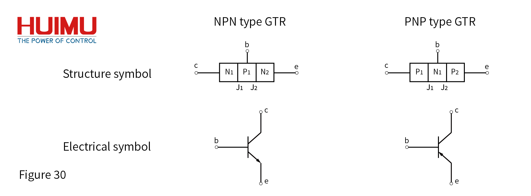
According to different structures, GTR can be divided into NPN type and PNP type (the following content takes NPN type GTR as an example). According to different structural forms, GTR can be divided into single-tube type GTR, Darlington type GTR (composite-tube type GTR) and GTR module. Single-tube type GTR has a low saturation voltage drop and a slightly fast switching speed, but the current gain β is small (usually around 10), the current capacity is small, and the drive power is large. It is generally used in small capacity inverter circuits. The Darlington type GTR has the advantages of large current gain β (usually up to tens or hundreds of times), large current capacity, small driving power consumption, but its saturation voltage drop is high, and the turn-off speed is slow.
The Darlington type GTR contains multiple units (each unit consists of a Darlington tube), and these units are connected in parallel through integrated circuit technology. The GTR module encapsulates two or more (4, 6, or even 7) single-tube type GTR or Darlington type GTR dies in a single tube case. The GTR tubes in the GTR module can form single bridge arm, single-phase bridge, three-phase bridge, and three-phase bridge with bleeder pipe. GTR module has the advantages of housing insulation, easy to design and install. At present, single-tube type GTR and non-modular Darlington type GTR are rarely used in inverter circuits, while GTR modules are still widely used.
* Darlington tube
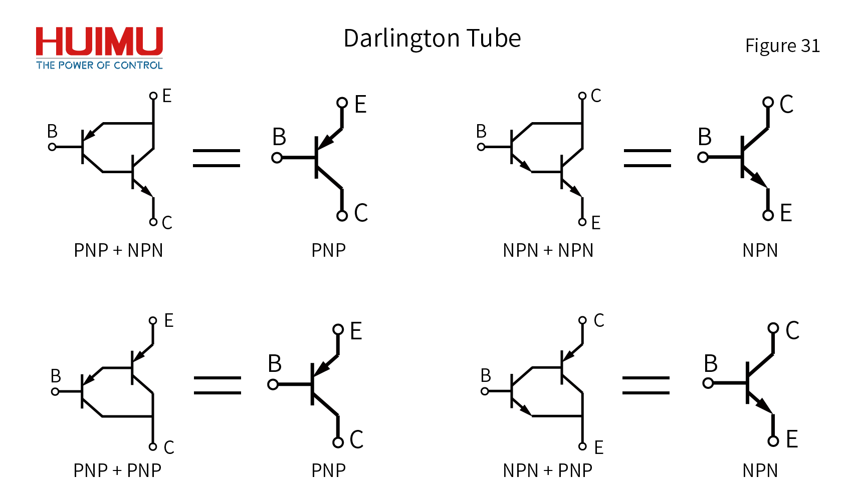
The Darlington tube is also called a composite tube. By connecting two transistors in series to form an equivalent transistor -- the output signal of the first transistor is used as the base signal of the second transistor. The type of equivalent transistor is the same as that of the first transistor. Both transistors are operated in the amplifying region by an appropriate external voltage, so the current gain of this equivalent transistor is the product of the current gains of the two transistors. Darlington tubes are usually used to amplify very tiny signals in highly sensitive amplifying circuits, such as high-power switching circuits, power amplifiers and regulated power supplies.
5.3.2 How does the GTR work?
5.3.2.1 Basic Structure of GTR
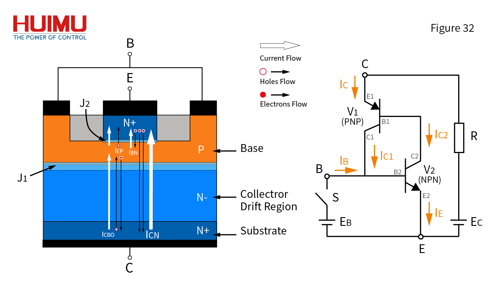
The structure of GTR is similar to the structure of BJT. NPN type GTR is divided into emitter region, base region and collector region by two PN junctions (collector junction J1 and emitter junction J2) -- the emitter region has small area and high doping concentration; the base region has thin thickness (5-20μm) and low doping concentration; the collector region is divided into two parts, the N- collector drift region has a large area and low doping concentration, and the N+ substrate region has small area and high doping concentration.
5.3.2.2 Working Principle of GTR
The working principle and calculation formula of GTR are the same as the working principle and calculation formula of BJT. However, it should be noted that during the turn-on process, the N+ substrate region will inject a large number of free electrons into the N- drift region to increase the reverse current of J1.
5.3.3 Main Parameters of GTR
Most of the parameters of GTR are the same as the main parameters of BJT.
1- Breakdown Voltage BV
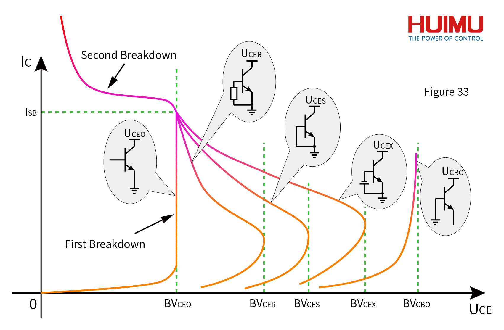
When the voltage UCE applied to the output of the GTR exceeds the specified value, the GTR will be broken down, and this voltage is called the breakdown voltage BV. The breakdown voltage is not only related to the characteristics of GTR, but also related to the connection method of the external circuit, as shown in Figure 33.
BVCBO is the reverse breakdown voltage between the collector and the base when the emitter is open;
BVCEO is the breakdown voltage between the collector and the emitter when the base is open;
BVCER is the breakdown voltage between the collector and the emitter when the emitter and the base are connected by a resistor;
BVCES is the breakdown voltage between the collector and the emitter when the emitter and the base are short-circuited;
BVCEX is the breakdown voltage between the collector and the emitter when the emitter junction is reverse biased.
These breakdown voltages have the following relationship:
BVCBO>BVCEX>BVCES>BVCER>BVCEO
To ensure safety, in the actual process, it is recommended that the maximum working voltage be much lower than BVCEO.
2- Maximum Collector-emitter Voltage UCEM
The maximum collector-emitter voltage UCEM is the rated voltage of GTR. In order to ensure safe use, the maximum operating voltage UCEM will be lower than the breakdown voltage BVCEO.
3- Second Breakdown Power PSB
The second breakdown mainly occurs in the case of high voltage and low current, and the corresponding second breakdown withstand capacity is called the second breakdown power PSB.
5.3.4 Basic Characteristics of GTR
5.3.4.1 Static Characteristics of GTR
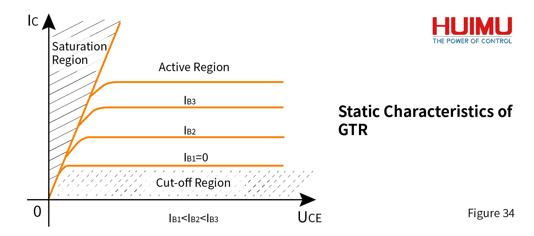
The static characteristics of GTR are similar to the static characteristics of BJT. The difference is that the low-current BJT will work in the amplification region, while the GTR only works in the saturation region and the cut-off region (that is, GTR has only on state and off state, and dose not have amplification state). It is because that when the GTR is working in the amplification state, its current is very large, and the power consumption is also large, which will make the GTR easily burned out due to severe heat. However, in the switching process (the process of switching back and forth from on state to off state), the GTR must cross the amplification region. Usually, this process will be very fast to avoid damage to the GTR.
5.3.4.2 Dynamic Characteristics of GTR
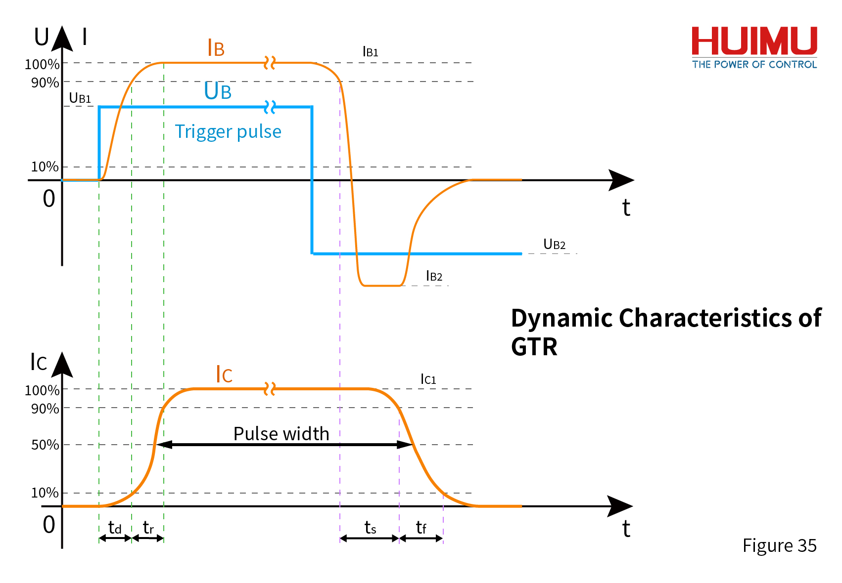
The dynamic characteristics of GTR are similar to the dynamic characteristics of BJT.
1- Turn-on Process
By applying a forward base current IB1, GTR will enter the conducting state. The turn-on process is divided into the delay time td and the rise time tr.
The calculation formula of turn-on time: ton = td + tr
2- Turn-off Process
By turning off the base current IB, GTR can be cut off. And a reverse current can speed up the turn-off process. The turn-off process is divided into the storage time ts and the fall time tf.
The calculation formula of the turn-off time: toff=ts + tf
* How to speed up the Turn-on Process of GTR
● Add an acceleration capacitor. By connecting a capacitor in parallel at both ends of the base resistance of the GTR, and using the feature that the capacitor voltage cannot change suddenly at the moment of commutation, to improve the switching characteristics of the GTR. Of course, a fast switch GTR tube with a relatively small junction capacitance can also be selected.
● Increase the drive speed. When the GTR is turned on, by providing a forward drive current with a certain amplitude and a steep front edge, td and tr can be reduced to accelerate the turn-on process of the GTR and shorten the turn-on time ton. However, the drive current cannot be too large, otherwise the diffusion time ts of the GTR will be increased due to oversaturation.
* How to speed up the Turn-off Process of GTR
● Reduce the saturation depth. By reducing the saturation depth during turn-on process, the carriers stored on the base can be reduced to shorten the storage time ts of the GTR.
● Apply negative drive current IB2. When the GTR is turned off, by applying a negative driving current with a certain amplitude and overshoot, the speed of extracting carriers from the base can be accelerated to shorten the storage time ts of the GTR.
● Apply reverse base voltage UB2. When the GTR is turned off, the dissipation of the stored charge can be accelerated by increasing the reverse base voltage to shorten the storage time ts of the GTR. But the reverse base voltage should not be too large to avoid breakdown of the emitter junction.
3- Second Breakdown Phenomenon of GTR
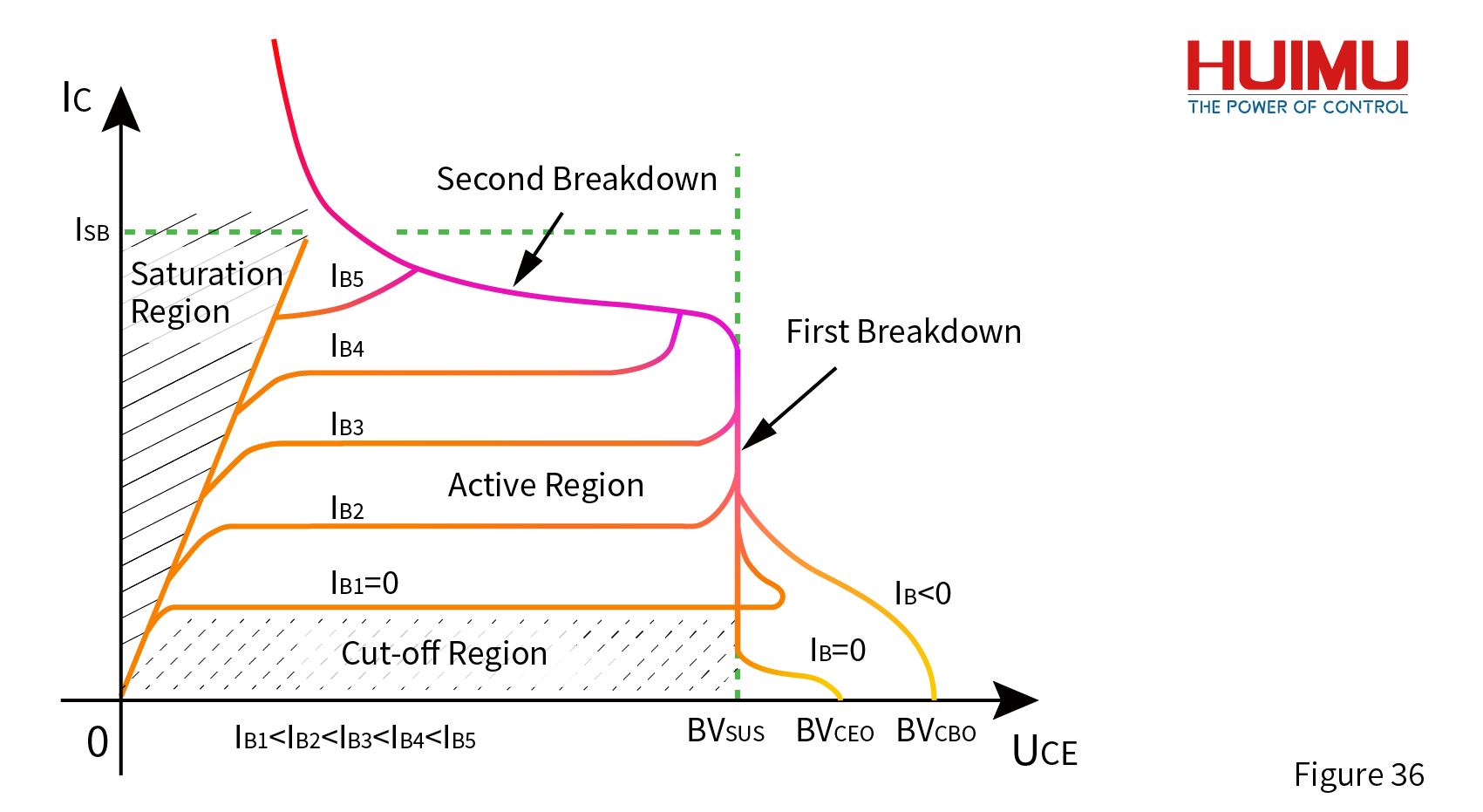
First Breakdown: When the collector voltage exceeds the breakdown voltage BVCEO, the GTR will be broken down -- IC increases rapidly, and the output voltage UCE of GTR will remain at a certain value (that is, the maintenance voltage BVsus). When the first breakdown occurs, as long as the external circuit can limit the current after the breakdown, the GTR will not be damaged. After the collector voltage is reduced to less than BVCEO, the GTR will return to normal, and its operating characteristics will not change. Therefore, the first breakdown is reversible and cannot cause damage to the GTR.
Second Breakdown: When the first breakdown occurs, if current limiting measures are not taken immediately, the collector current IC will reach the critical point of second breakdown ISB, which will cause the local current density in the GTR to increase. The local area will heat up and further increasing the local current density. After a series of positive feedback, although the surface temperature of the GTR is not high, the local area inside it is damaged due to the high temperature, and a low resistance channel is formed between the collector and the emitter, and the collector voltage UCE drops, and the collector current IC rises sharply. This phenomenon is called second breakdown. The second breakdown is irreversible, it will cause permanent damage to the GTR and significantly degrade its working characteristics.
4- Safe Operating Area of GTR
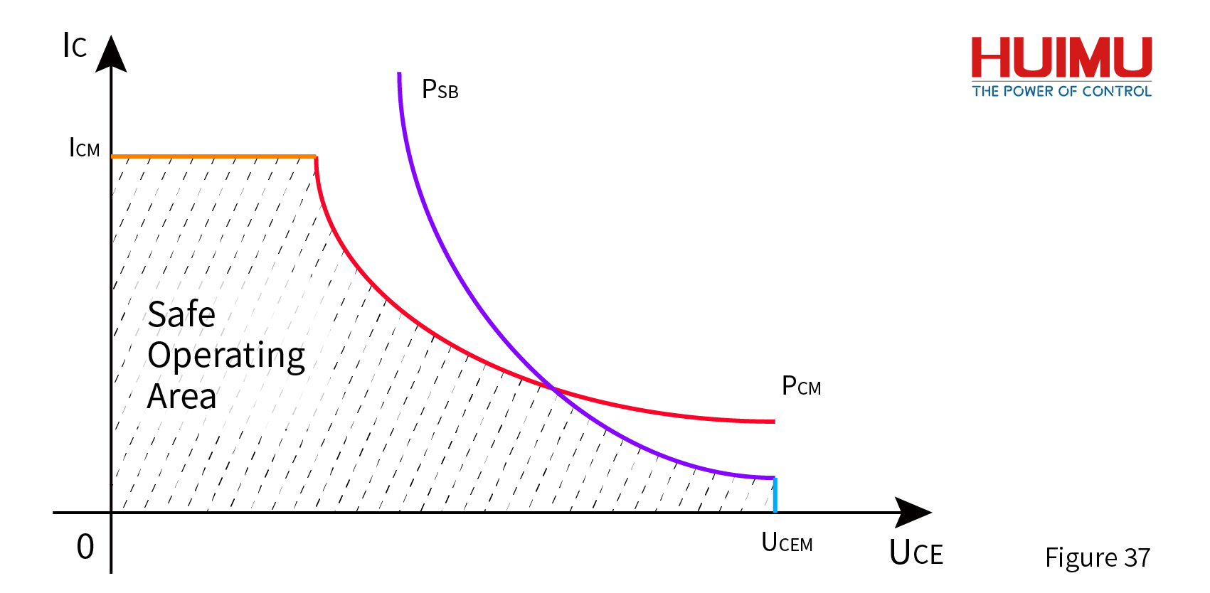
The maximum voltage UCEM, the maximum collector current ICM, the maximum dissipation power PCM, and the second breakdown power PSB constitute the second breakdown critical line. The area marked by the shadow in the second breakdown critical line is the safe operating area.
5.4 Power MOSFET
5.4.1 Introduction to MOSFET
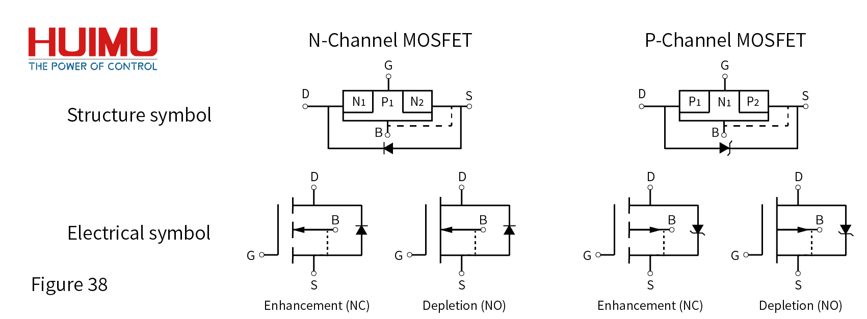
The field effect transistor (FET) is a unipolar device controlled by voltage. The working principle of FET is mainly to use an electric field to form a conductive channel in a semiconductor to control the conductivity of the semiconductor. FET can be divided into junction FET (JFET, also known as static induction transistor, SIT) and insulated gate FET.
The metal-oxide-semiconductor field effect transistor (MOSFET) is an insulated gate field effect transistor made of metal, oxide and semiconductor. MOSFET is a very important power electronic device. MOSFET has high input impedance (about 107-1015Ω), low noise, low power consumption, large dynamic range, good temperature characteristics, easy to integrate, no second breakdown phenomenon, simple drive circuit, small drive power, fast switching speed, high operating frequency, good thermal stability (better than GTR), wide safe operating area, and the gate bias can be positive or negative or zero. Because of these advantages, MOSFETs are widely used in circuits, such as signal amplification, impedance conversion, variable resistors, constant current sources, electronic switches, and etc. Compared with other power electronic devices, due to the small current capacity and the low withstand voltage of MOSFET, a multi-unit integrated mechanism is usually used to form the Power MOSFET with high power capacity, which is mostly used in high-frequency power electronic equipment below 1kW. MOSFETs are mainly used in DC solid state relays (click to view more DC solid state relays ).
5.4.2 How does the MOSFET work?
5.4.2.1 Basic Structure of MOSFET
MOSFET has four terminals -- gate (G), drain (D), source (S), and body (B). The main structure of the MOSFET is a substrate (also called body or base), whose main material is silicon. There is an oxide insulating layer (also called a gate oxide layer or a gate insulating layer) between the source and the drain, whose material is normally SiO2. The gate is on the gate insulating layer, whose material is used to be aluminum (aluminum gate), but now is polysilicon (poly-silicon gate). The internal resistance of the gate of the MOSFET is extremely high (up to several hundred megaohms), so there is no conduction between the gate, the source, the drain, and the substrate. In actual use, a power diode is usually connected in parallel between the drain and source of the MOSFET to avoid the instantaneous reverse current in the circuit from breaking down the MOSFET. Generally, the power diode is directly integrated into the MOSFET.
According to the material of the substrate, MOSFET can be divided into N-MOSFET (or N-MOS) and P-MOSFET (or P-MOS). N-MOS uses a P-type substrate, and its source must be connected to the lowest potential of the circuit; P-MOS uses an N-type substrate, and its source must be connected to the highest potential of the circuit.
According to whether there is a conductive channel between the source and drain when the gate voltage is zero, MOSFETs can be divided into enhancement type MOSFET and depletion type MOSFET.
According to whether the source and drain are on the same plane, the structure of the MOSFET can be divided into a vertical structure and a horizontal structure.
There are many branch types and derivative devices of MOSFET, which cannot be listed here. The following is an introduction to LDMOSFET, CMOS and VDMOSFET.
1- LDMOSFET
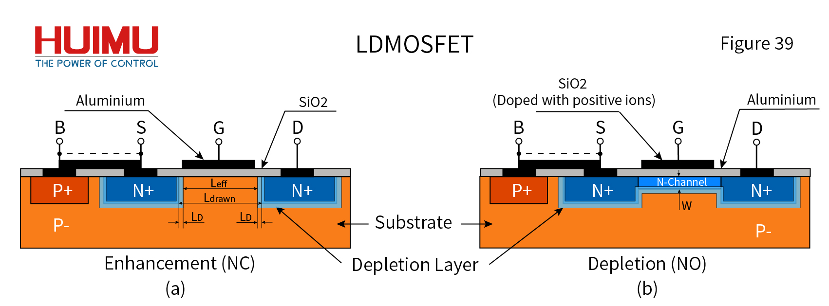
The source (S) and drain (D) of the LDMOSFET are on the same plane, so a separate body (B) is required. Take N-channel LDMOSFET as an example (as shown in Figure 39). Its substrate is a P- substrate region, and the carriers involved in conduction are free electrons. There are two highly doped N+ regions in the P- substate region (P- Sub), one of which is called the source region and the other is called the drain region. These two regions are exactly the same, and theoretically it is no problem to swap them. Since the source (S) and drain (D) are on the same plane, the threshold voltage shift caused by the body effect is prone to occur. Therefore, by adding a high-doped P+ region to the P- substrate region, the body (B) is connected to the source (S) from the P+ region, so that the potential of the body is equal to the potential of the source, and the body effect can be avoided. The conductive channel in the LDMOSFET is formed in the substrate -- when the gate voltage of the enhanced N-channel LDMOSFET is 0, there is no channel between the source and the drain, as shown in Figure 39, a; when the gate voltage of the depletion N-channel LDMOSFET is 0, there is a channel between the source and the drain, as shown in Figure 39, b. By increasing the lateral dimension (horizontal area), the channel length of LDMOSFET increases. However, the increase of the horizontal area will lead to the increase of the on-resistance of LDMOSFET.
* Length and Width of the Conductive Channel
The distance between the source region and the drain region is called the conductive channel length. Ldrawn = Leff + 2 * LD. Ldrawn is the total channel length, Leff is the effective channel length, and LD is the lateral diffusion length. The distance from the gate to the bottom of the conductive channel is called the conductive channel width. The length (L) and width (W) of the conductive channel determine the channel resistance of the MOSFET.
* Body Effect
Body effect refers to that the width of the depletion region at the conductive channel is wider after the substrate voltage is lower than the source voltage, which will result in a higher threshold voltage.
2- CMOS
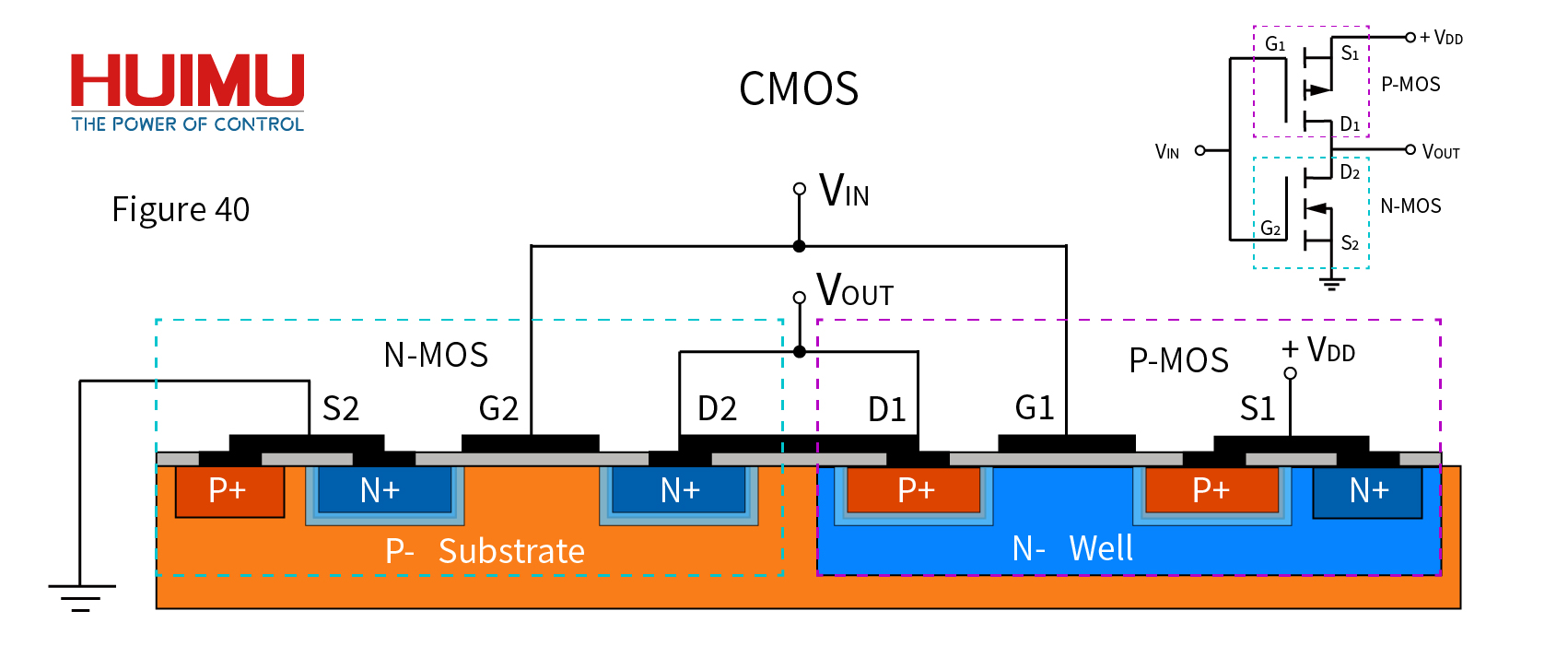
CMOS is one of the most commonly used processes in integrated circuits. It can integrate multiple N-MOS and P-MOS on a single silicon chip. P-MOS is directly embedded in N-MOS, so the substrate of P-MOS is also called N- Well. CMOS has the advantages of high efficiency, low power consumption, high impedance, and the ability to process complex logic.
3- VDMOSFET
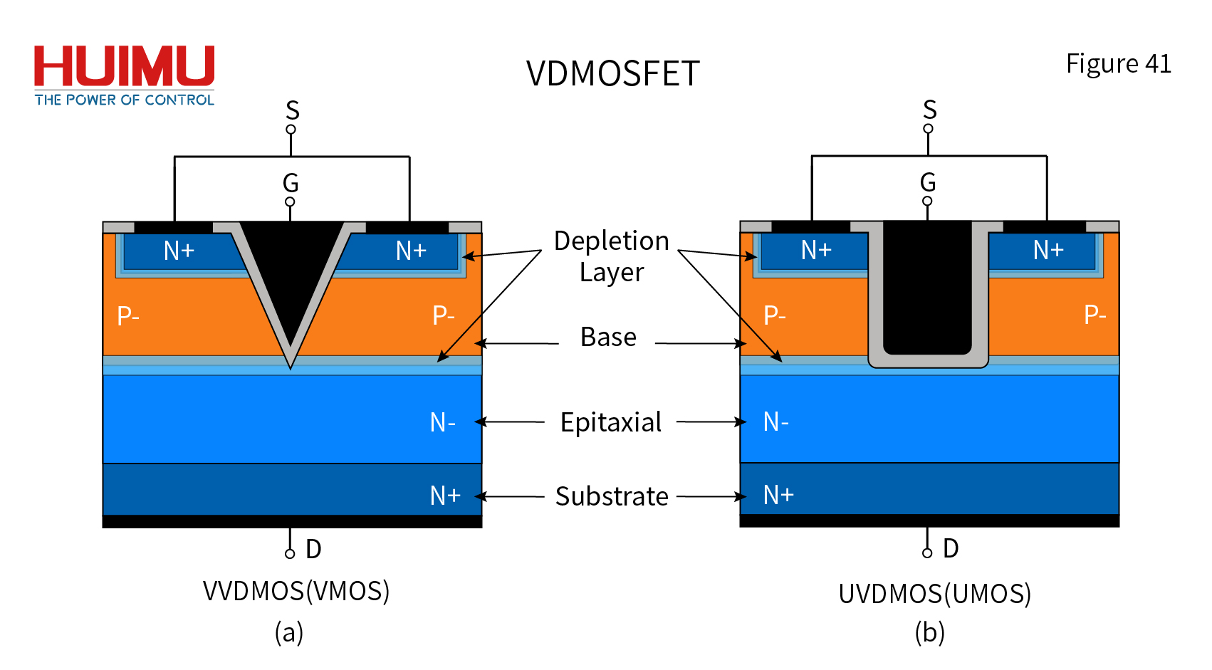
The vertical double-diffused MOSFET (VDMOSFET) is the most common power MOSFET (Figure 41 shows the enhanced N-channel VDMOSFET). The source and drain of the VDMOSFET are not on the same plane, so a separate body (B) is not required. By increasing the vertical dimension (vertical area) without increasing the horizontal area, the channel length of VDMOSFET increases. Therefore, for MOSFETs with the same on-resistance, VDMOSFET has higher current withstand capabilities than LDMOSFET. Because there is an extra layer of N- epitaxial region with low doping concentration between the P region and the N region of VDMOSFET, which increase the equivalent resistance of the VDMOSFET, so VDMOSFET can withstand a higher voltage. Although due to the conductance modulation effect, when the current flowing through the PN junction gradually increases, the internal resistance of the N- epitaxial region will decrease, but the voltage withstand capability of the VDMOSFET is still greater than that of the LDMOSFET. In addition, the N region and the P region form a parasitic power diode, which can effectively protect the VDMOSFET from reverse voltage breakdown. Therefore, most power MOSFETs adopt a vertical structure to obtain better withstand voltage and current capability.
According to the shape of the groove gate, VDMOSFET can be divided into VVDMOS (also known as v-groove vertical double-diffused MOSFET, or v-groove vertical channel double diffused MOSFET, VMOS) and UVDMOS (also known as u-groove vertical double-diffused MOSFET, or u-groove vertical channel double diffused MOSFET, UMOS). UMOS has a better withstand voltage capability than VMOS. Since VMOS is very widely used in the field of power electronics, generally power MOSFET refers to VMOS.
5.4.2.3 Working Principle of MOSFET
The working principle of MOSFET is to change the conductivity inside the semiconductor by applying an external electric field. The working principle of P-MOSFET is exactly the same as that of N-MOSFET. In addition, the working principles of VDMOSFET and LDMOSFET are similar, but the lateral structure facilitates clear observation of current changes inside the MOSFET. So, the following takes the N-channel LDMOSFET as example to introduce the working principle of MOSFET.
1- Enhancement Type MOSFET
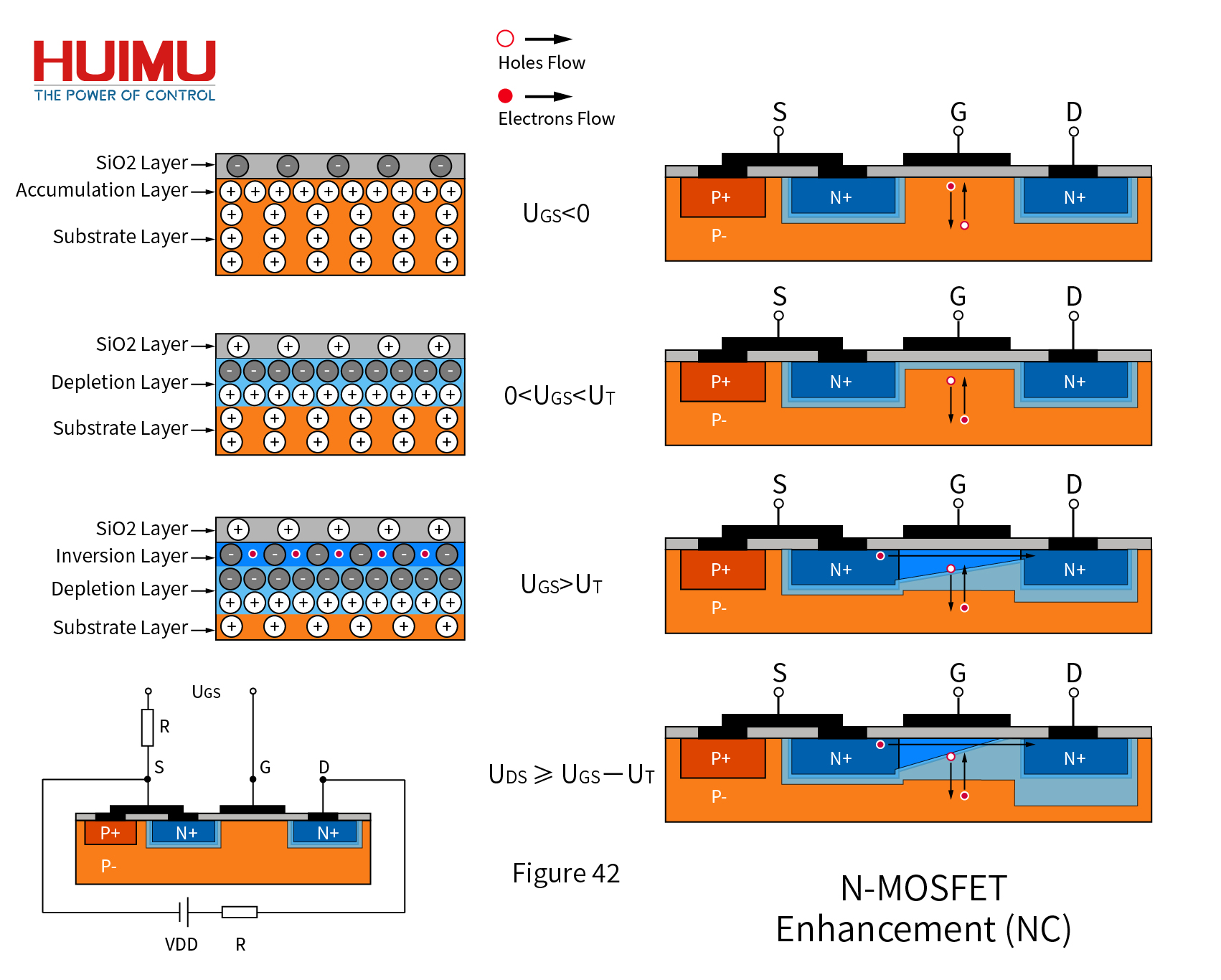
When the gate voltage is not applied (UGS=0), there is no conductive channel between the source region and the drain region of the enhancement type MOSFET, and the conductive channel will be formed only after a certain gate voltage is applied. Therefore, the enhancement type MOSFET is a normally closed (NC) device.
Accumulation Layer Stage: When UGS<0, an electric field perpendicular to the semiconductor surface will be generated at the gate, which will attract holes in the P- region to the bottom of the insulating layer and repel the free electrons in the P- region, and then form an accumulation layer. Even if a positive voltage is applied between the source and the drain, current cannot flow directly from the drain to the source (the leakage current is not considered), so the MOSFET is in the off state.
Depletion Layer Stage: When 0<UGS<UT, an electric field perpendicular to the semiconductor surface will be generated at the gate, which will attract free electrons in the P- region to the bottom of the insulating layer and repel the holes in the P- region, and then form a depletion layer. However, because the free electrons accumulated at the bottom of the insulating layer are too few to form a conductive channel, the MOSFET is still in the off state.
Inversion Layer Stage: When UGS≥UT, the free electrons accumulated at the bottom of the insulating layer is enough to form an N type narrow layer (that is, N type conductive channel). Since the type of the N type conductive channel is opposite to that of the P- region, it is also called an inversion layer. The existence of the conductive channel allows current to flow from the drain region to the source region, so the MOSFET is in the on state. With the increase of UGS, the stronger the electric field formed by the gate, the more free electrons are attracted to the bottom of the insulating layer, the wider the conductive channel, the smaller the channel resistance, and the larger the drain current ID. It should be noted that the voltage drop generated by the drain current ID along the channel makes the voltage between each point in the channel and the gate no longer equal -- the closer to the source region, the greater the voltage drop and the wider the channel; the closer to the drain region, the smaller the voltage drop and the narrower the channel. The voltage drop at the end closest to the drain region is the smallest (its value is UGD= UGS - UDS), the channel is the narrowest. And as UDS increases, the channel near the drain region becomes narrower and narrower.
Pinch-off Region Stage: When the MOSFET is turned on, if UDS keeps increasing until UGD = UGS - UDS = UT, the channel width of the end closest to the drain region becomes 0, and a strong inversion channel cannot be formed, that is, the channel is pinched off. The point on the channel with a width of 0 is called the pinch-off point, and the depletion region between the pinch-off point and the drain region is called the pinch-off region. If UDS continue to increase, the pinch-off point will move to the source region. Since the increase of UDS is almost applied to the pinch-off region, the pinch-off region will also continue to expand. After the channel is pinched off, even if the drain voltage continues to increase, the drain current remains at a constant value (that is, the saturated drain current ID(sat)), and the MOSFET is in a saturation state. The saturated drain current ID(sat) is not affected by UDS, but is determined by UGS -- ID(sat) has a relationship with the square of UGS, which is the MOSFET square-law transfer characteristics.
2- Depletion Type MOSFET
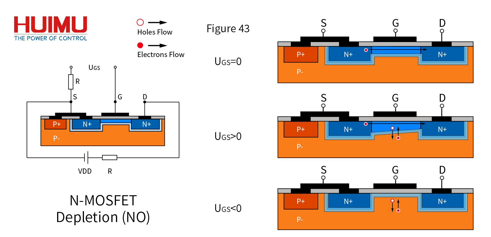
When the gate voltage is not applied (UGS=0), there is a conductive channel between the source region and the drain region of the depletion MOSFET. When a forward gate voltage is applied, the width of the conductive channel will increase. When the reverse gate voltage is applied, the width of the conductive channel will decrease. When the reverse gate voltage reaches a certain value, the conductive channel disappears. Therefore, the depletion N-MOSFET is a normally opened (NO) device.
Conduction State: When UGS≥0, the electric field generated on the gate will attract more electrons to the N channel and repel the holes in the N channel. As UGS increases, the channel becomes wider, the channel resistance becomes smaller, and ID increases.
Cut-off State: When UGS<0, the electric field generated on the gate will attract more holes to the N channel and repel the electrons in the N channel, making the channel narrower and the channel resistance larger. When UGS reaches the pinch-off voltage UPO, the electrons in the N channel are depleted, the conductive channel disappears, and ID tends to zero.
5.4.3 Main Parameters of MOSFET
Most of the parameters of MOSFET are the same as the main parameters of BJT.
1- Transconductance Gfs
Generally speaking, the ratio of the input current to the input voltage is called admittance. Due to the transfer characteristics of MOSFET, its gate-source input voltage UGS does not affect the change of gate-source input current IGS, but affects the change of drain current iD, so the ratio of the drain current ID to the gate-source voltage UGS is called transconductance.
2- Parasitic Capacitance
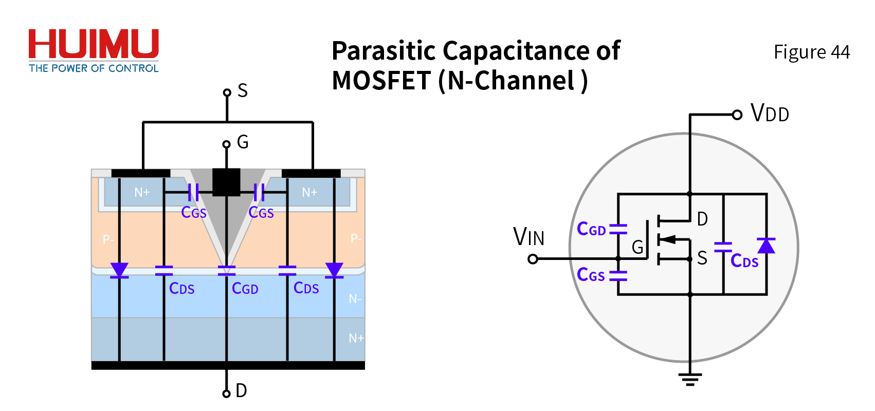
There are three internal parasitic capacitances inside the MOSFET: The gate-source parasitic capacitance CGS, the gate-drain parasitic capacitance CGD (also known as Miller capacitance), and the drain-source parasitic capacitance CDS. These parasitic capacitances will affect the dynamic characteristics of the MOSFET -- if the parasitic capacitance is small, the switching current and the driving power are small, and the switching speed is fast; if the parasitic capacitance is large, the switching current and the driving power are large, and the switching speed is slow. MOSFET manufacturers usually give the capacitance parameters of the MOSFET, which meet the following calculation formulas:
Input capacitance of MOSFET: Ciss = CGS + CGD
Output capacitance of MOSFET: Coss = CDS + CGD
Reverse transfer capacitance of MOSFET: Crss = CGD
3- Drain-source On-resistance RDS(on)
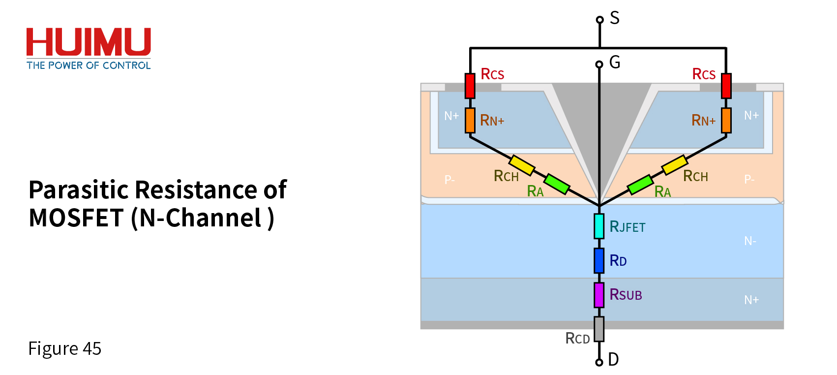
The drain-source on-resistance RDS(on) refers to the on-resistance between the drain and source of the MOSFET when it is turned on under certain conditions. RDS(on) is determined by the parasitic resistance of MOSFET, RDS(on) = RCS + RN+ + RCH + RA + RJFET + RD + RSUB + RCD. RCS is the contact resistance between the N+ source region and the source electrode; RN+ is the resistance between the N+ source region and the channel; RCH is the resistance of the channel; RA Is the resistance of the accumulation layer; RJFET is the resistance of the equivalent JFET; RD is the resistance of the drift region; RSUB is the resistance of the substrate region; RCD is the contact resistance between the substrate region and the drain electrode. The drain-source on-resistance RDS(on) is affected by the MOSFET junction temperature and the gate-source voltage (driving voltage) UGS. The higher the junction temperature, the larger RDS(on); on the contrary, the smaller RDS(on). The higher the gate-source voltage, the smaller RDS(on); on the contrary, the larger RDS(on).
4- Maximum Drain Current IDM
The maximum drain current IDM is the rated current of the MOSFET. The maximum drain current refers to the drain current that enables the MOSFET to reach the highest junction temperature when the case temperature is at a certain value. The maximum drain current is not only related to the structure of the MOSFET, but also related to the packaging method of the MOSFET and the ambient temperature.
5- Maximum Drain-source Voltage BVDSS
The maximum drain-source voltage BVDSS is the rated voltage of the MOSFET. The maximum drain-source voltage refers to the maximum voltage that can be applied when the MOSFET drain and source do not undergo avalanche breakdown when the ambient temperature is 25°C. In actual operation, the measured drain-source voltage value when the drain current is 250μA is usually taken as the maximum drain-source voltage BVDSS.
6- Maximum Gate-source Voltage UGSM
The maximum gate-source voltage (also known as the maximum driving voltage) refers to the maximum input voltage that can cause permanent damage to the gate insulating layer of the MOSFET in a very short time. It is generally recommended that the driving voltage should not exceed ±20V.
7- Switching Frequency
The switching time of MOSFET is between 10-100μs, and the operating frequency can reach above 100kHz (even up to several MHz), which is the highest among major power electronic devices. Although the MOSFET hardly needs input current when it is static, it will charge and discharge the parasitic capacitance when it is dynamic (switching process), so a certain drive power is still required. The higher the switching frequency of the MOSFET, the greater the drive power required.
5.4.4 Basic Characteristics of MOSFET
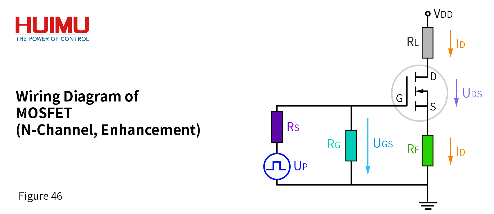
Take the enhanced N-MOSFET as an example. VDD is the output power source of MOSFET; UP is the driving signal source of MOSFET; UGS is the voltage between the gate and source; UDS is the output voltage drop of the MOSFET; ID is the drain current; RS is the internal resistance of the drive circuit; RG is the gate internal resistance; RL is the drain load; RF is the detection resistance, used to detect the drain current.
5.4.4.1 Static Characteristics of MOSFET
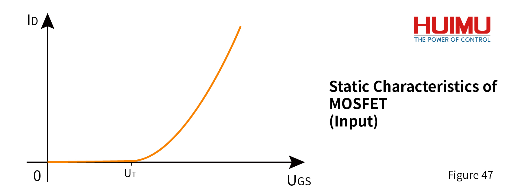
Due to the transfer characteristics of the MOSFET, the voltage change between the gate and source of the MOSFET will not affect the current between the gate and source, but it will affect the drain current ID. When ID is large, the relationship between ID and UGS is approximately linear, and its slope is the transconductance Gfs of the MOSFET.
2- Output Characteristics
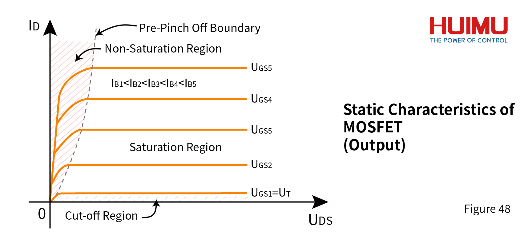
The static output characteristic curve of MOSFET is similar to the static output characteristic curve of GTR. The static output characteristic of MOSFET can be divided into cut-off region, saturation region and non-saturation region. MOSFET usually only works in the switching state (that is, fast switching back and forth between the cut-off region and the non-saturation region) to prevent the MOSFET from being burned out due to excessive power consumption when working in the saturation region.
Cut-off Region: Similar to the cut-off region of BJT. Although UDS is very high, the drain current ID=0 (the leakage current is not considered).
Saturation Region: Similar to the active region of BJT. ID is not affected by UDS, but increases with the increase of UGS. In the saturation region, the voltage and current that the MOSFET bears are large, so its power consumption is very large.
Non-saturation Region: Similar to the saturation region of BJT. ID increases with the increase of UDS. In the non-saturation, the MOSFET bears a large current and a very small voltage, so its power consumption is small. Because MOSFET behaves as a voltage-controlled resistor in the non-saturation region, so this region is also known as ohmic region or variable resistance region.
5.4.4.2 Dynamic Characteristics of MOSFET
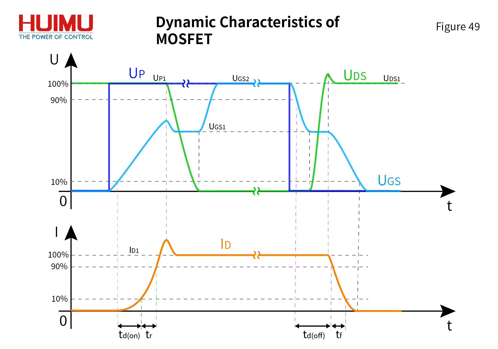
In the switching process of MOSFET, the influence of the internal parasitic capacitance on its switching time cannot be ignored.
1- Turn-on Process
In order to switch the MOSFET to the on-state, a steep input power source UP1 must be applied to its gate. Due to the existence of the internal resistance RS of the driving circuit and the gate-source parasitic capacitance CGS, the gate voltage UGS of the MOSFET cannot form a pulse waveform as steep as UP1, but rises with a certain slope. When the driving current starts to charge CGS so that UGS reaches UT, the MOSFET enters the on state, and the drain current ID starts to rise. When CGS is fully charged, UGS is maintained at UGS1, and ID is maintained at ID1. At this time, the drain-source parasitic capacitance CDS starts to discharge, and UDS starts decrease. When UDS reaches the minimum value, the driving current starts to charge the gate-drain parasitic capacitance CGD, and UGS rises again until it remains at UGS2. Generally, the time from UGS rising to 10% UGS2 to ID rising to 10% ID1 is called the turn-on delay time td(on). The time taken for ID to rise from 10% ID1 to 90% ID1 is called the rise time tr. The turn-on time ton of the MOSFET is the sum of the turn-on delay time td(on) and the rise time tr.
The calculation formula of the turn-on time: ton = td(on) + tr
2- Turn-off Process
When the driving pulse signal UP1 is removed, because of RS and CGD, UGS decreases with a certain slope. When CGD is discharged, UGS remains at UGS1, at this time, CDS starts to charge, and UDS starts to rise. When CDS is fully charged, UDS remains at 100% UDS1, at this time, CGS starts to discharge, and UGS drops again. When UGS drops below UT, the MOSFET enters the off state, and ID drops to 0. Since the MOSFET does not have a minority carrier storage effect, its turn-off process is very fast (about tens of nanoseconds). Generally, the time from 90% UGS2 to 90% ID1 is called the turn-off delay time td(off). The time it takes for ID to fall from 90% ID1 to 10% ID1 is called the fall time tf. The turn-off time ton of the MOSFET is the sum of the turn-off delay time td(off) and the fall time tf.
The calculation formula of the turn-off time: toff = td(off) + tf
* How to speed up the Switch Process of MOSFET
● Using a drive circuit with low internal resistance and inductance can speed up the turn-on process of the MOSFET.
● Improve the MOSFET's ability to charge and discharge the parasitic capacitance during the turn-on and turn-off process, which can effectively reduce the delay time, so that no transient error occurs.
5.4.5 Series and Parallel Connection of MOSFET
Because the switching speed of MOSFET is very fast, and its dynamic characteristics have a certain degree of dispersion, it is impossible to adopt common voltage equalization schemes. If MOSFETs connected in series, during the switching process, the working state of each MOSFET is different, and its withstand voltage capability cannot be kept the same, so it is easy to cause the MOSFET with low withstand voltage to burn out due to overvoltage. Therefore, MOSFETs are not suitable for series connection.
The on-resistance of the MOSFET has a positive temperature coefficient -- the higher the temperature, the greater the on-resistance. In practical applications, multiple MOSFETs can be used in parallel, for example, the output circuit of the inverter welding machine will connect dozens of MOSFETs in parallel to increase its current capacity. When one of the MOSFETs passes too much current, the greater the on-resistance, the more current will flow into other MOSFETs with smaller on-resistance, and finally the current flowing in each MOSFET tends to be balanced. The following methods can effectively reduce the phenomenon of uneven current: Select MOSFETs with small parameter error; the wiring and layout of the circuit should be symmetrical; the line loss (the resistance of the wire itself will consume current) and the inductance and capacitance of the wire under high frequency should be considered. It should be noted that connecting a small inductor in the source circuit can act as a current-sharing reactor, which can effectively reduce the dynamic uneven current, but it is invalid for the static uneven current.
5.5 Insulated-Gate Bipolar Transistor
5.5.1 Introduction to IGBT
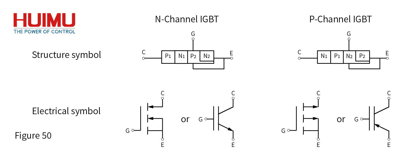
The insulated-gate bipolar transistor (IGBT, or IGT) is a composite Bi-MOS device with the high input impedance of Power MOSFET and the high current capacity of BJT. IGBT is widely used in many fields, such as converters, inverters, pulse width modulation systems (PWM), uninterruptible power supplies (UPS), switching mode power supplies (SMPS), resonant converters, industrial motors, new energy vehicles, etc. IGBT has the advantages of high input impedance, low noise, fast switching speed, simple driving circuit, low driving power, low on-state voltage, low switching loss, wide safe operating area, small size, high current density, high current capacity, high endurance voltage, strong resistance to pulse current impact, and no second breakdown. Compared to Power MOSFET, IGBT has the disadvantages of slow switching speed and easy to latch-up. IGBT is mainly used in fields where the withstand voltage is above 600V, the current is above 10A, and the frequency is above 1kHz.
5.5.2 How does the IGBT work?
5.5.2.1 Basic Structure of IGBT
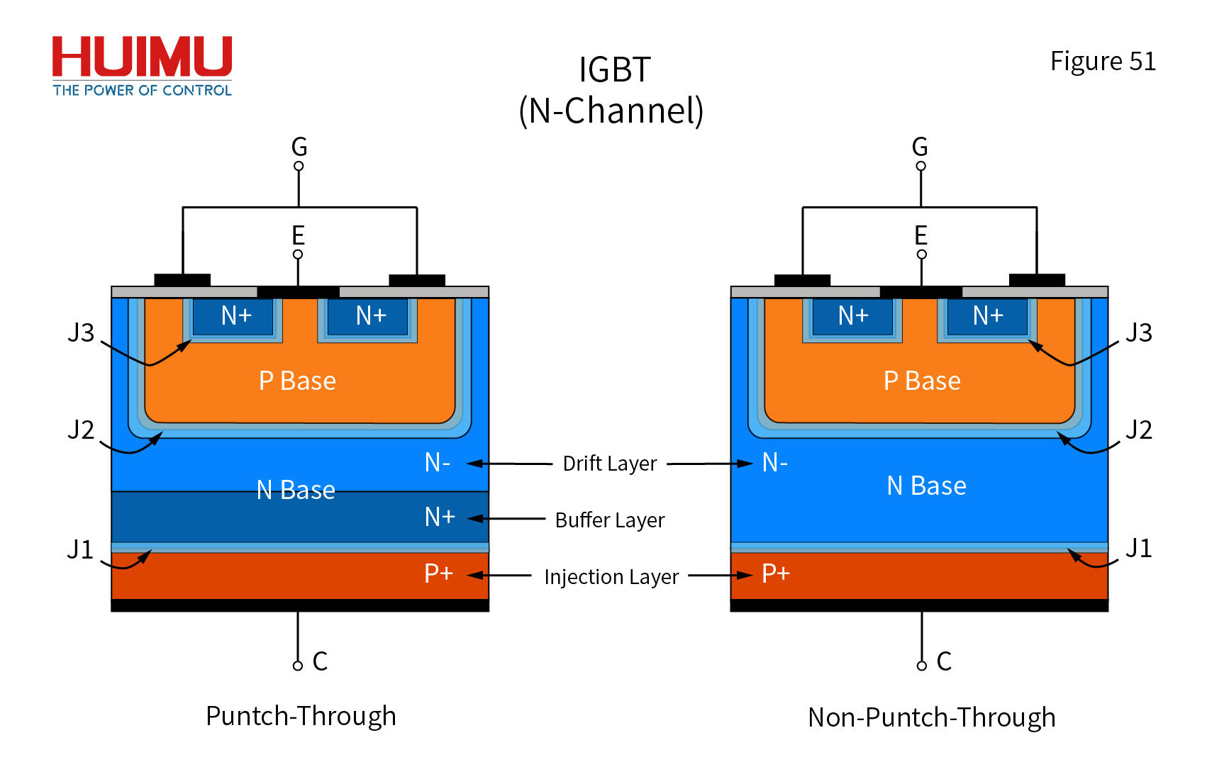
The structure of IGBT is very similar to that of Power MOSFET -- the gate (G) of the IGBT corresponds to the gate (G) of the MOSFET; the emitter (E) of the IGBT corresponds to the source (S) of the MOSFET; the collector (C) of the IGBT corresponds to the drain (D) of MOSFET. However, IGBT has a P+ injection layer in substrate region which makes the IGBT become a P-N-P-N structure like a thyristor. According to whether it contains N+ buffer layer, IGBT can be divided into Punch-Through type (PT) and Non-Punch-Through type (NPT). PT type IGBT has the advantages of low switching loss, low on-state loss, and large current capacity, but its temperature characteristic is not as good as NPT, and it is not suitable for parallel connection. The forward breakdown voltage of PT type IGBT is higher than the reverse breakdown voltage, so it is more suitable for DC circuits; the forward breakdown voltage of NPT type IGBT is the same as the reverse breakdown voltage, so it is more suitable for AC circuits. Since the switching speed of P-Channel IGBT is 2-3 times slower than that of N-Channel IGBT, the safe operating area (SOA) of P-Channel IGBT is smaller than that of N-Channel IGBT, and the cost of P-Channel IGBT is higher than that of N-Channel IGBT, so P-Channel IGBT is rare in actual use. The following mainly introduces PT type N-Channel IGBT.
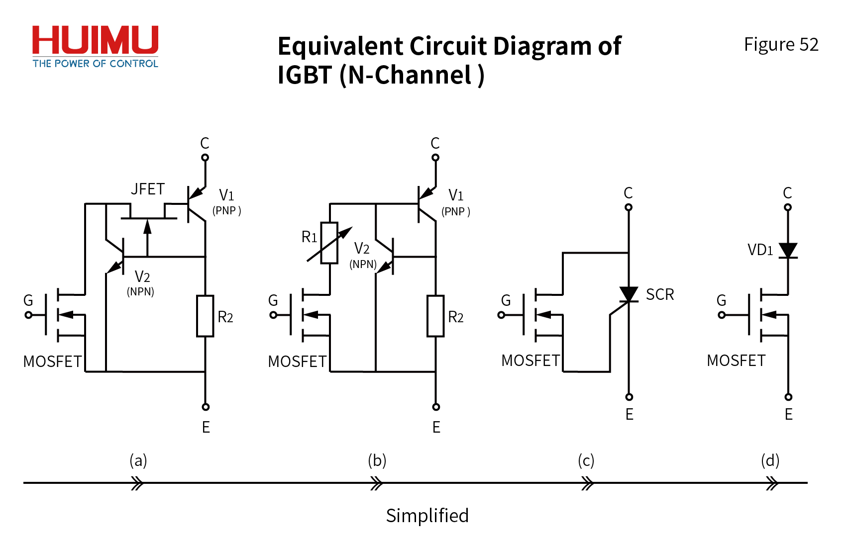
The equivalent circuit diagram of the PT type N-Channel IGBT is a circuit that composed of a parasitic enhancement N-MOSFET, a parasitic JFET, a parasitic PNP transistor V1 (P+ N- P), and a parasitic NPN transistor V2 (N+ P N-), and an equivalent extended resistance R2, as shown in Figure 51, a. In this circuit, V1 is the main output channel; V2 is formed with the formation of MOSFT; JFET is mainly formed by the N- drift region; R2 is mainly formed by the equivalent resistance of the P base region of V2. The parasitic JFET can be further simplified as the equivalent modulation resistance R1 which is mainly formed by the equivalent resistance of the N- drift region. And then the equivalent circuit diagram of the IGBT can be simplified as shown in Figure 51, b. The four-layer semiconductor structure (P-N-P-N) of the IGBT can be regarded as a parasitic thyristor SCR, and the equivalent circuit diagram of the IGBT can be further simplified as shown in Figure 51, c. If the IGBT is regarded as a MOSFET with large current switching capability, the P+ and N+ regions can be regarded as a power diode VD1, and the equivalent circuit diagram of the IGBT can be further simplified as shown in Figure 51, d. The simplified equivalent circuit diagram helps to intuitively understand the working principle of the IGBT.
5.5.2.2 Working Principle of IGBT
In simple terms, the working principle of IGBT is a voltage-drive thyristor.
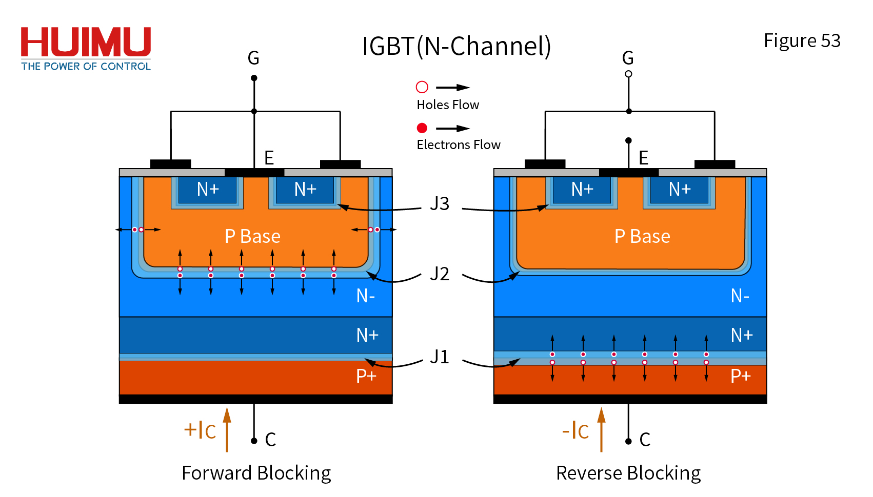
Forward Blocking State: When a forward voltage is applied to the IGBT and the gate and emitter are short-circuited, the IGBT will enter a forward blocking state. At this time, the PN junctions J1 and J3 are forward biased, and the PN junction J2 is reverse bias. The reverse voltage makes the depletion layer on both sides of J2 extend to the P base region and the N-drift region.
Reverse Blocking State: When a reverse voltage is applied to the IGBT, the PN junction J1 is reverse biased, and the reverse voltage makes the depletion layer of J1 extend to the N- buffer region. By increasing the width of the N- buffer region, the reverse blocking capability of the IGBT can be improved, but it will also increase the forward voltage drop of the IGBT. The reverse withstand voltage of IGBT is usually only a few tens of volts, so in order to prevent the IGBT from working in the reverse blocking state, a FRED is connected in anti-parallel to the IGBT. Of course, for convenience, IGBT and FRED will be packaged together to form an reverse-conducting IGBT module.
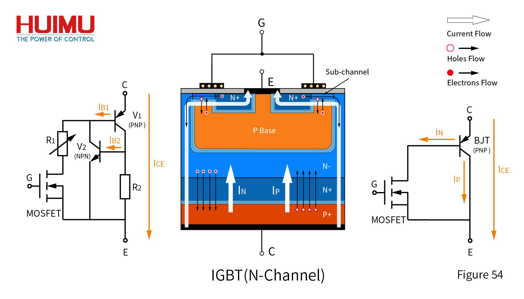
Conduction State: When a forward voltage is applied to the IGBT and a certain voltage is applied to the gate, the P base region will form a N sub-channel region, allowing electrons to be transferred from the N+ emitter region to the N- drift region. This electrons flow will reduce the potential of the N base region and provide the base current IB1 for V1. If the voltage drop generated by this electrons flow is about 0.7V, then the PN junction J1 will be forward biased, and the IGBT start to be turned on. The N- drift region of IGBT is very wide and the doping concentration is low, so the N- drift region has a very low conductivity. When the IGBT is working at high current, due to the conductance modulation effect, the carrier concentration of the N- base region increases and its conductivity increases, which will reduce the saturation voltage between the collector and the emitter and the total on-state power consumption of the IGBT. When there are electron current IN and hole current IP, the IGBT is completely turned on. When the IGBT is in the on state, its collector current should be limited to avoid latch-up effect.
Cut-off State: When the gate voltage UGE is lower than the threshold voltage UT or a reverse bias voltage is applied to the gate, the N sub-channel disappears, the base current in the IGBT is cut off, and then IN and IP disappear, IGBT enters the cut-off state. However, due to the minority carrier effect, the IGBT output current will not be reduced to zero immediately, but a tail current will be generated like BJT, whose characteristics are related to UCE, IC and TC. The minority carrier effect will increase the switching time and switching loss of the IGBT.
* Latch-up Effect
Usually, R2 will short-circuit the base and emitter of V2 to prevent V2 from working. When the current flowing through R2 is too large, so that the forward voltage drop on R2 is sufficient to provide the trigger current IB2 for V2, then V1 and V2 will form a equivalent thyristor SCR (P+ N- P N+). Due to the positive feedback mechanism inside the equivalent thyristor, V1 and V2 will enter a deep saturation state, so the channel of IGBT is difficult to be shut off by the gate voltage, and IGBT can be shut off only if a very large reverse voltage is applied. This phenomenon is called the latch-up effect, which can be divided into static latch-up and dynamic latch-up. The static latch-up is caused by the excessive collector current IC when the equivalent thyristor is completely turned on. The dynamic latch-up is caused by the large displacement current caused by excessive di/dt and dv/dt during the switching process of IGBT. The collector current that causes the dynamic latch-up is smaller than that of the static latch-up. The latch-up effect makes V1 and V2 form a Darlington structure, so IC and power consumption of the IGBT will increase significantly, which will damage the IGBT. The following measures are usually taken to avoid the latch-up effect:
● Reduce R2 by changing the internal structure and doping of the IGBT to prevent V2 from turning on.
● By optimizing the width and doping of the N- buffer layer to reduce the current gain α of V1 (generally less than 0.5) to suppress the work of V2.
5.5.3 Main Parameters of IGBT
Most of the parameters of IGBT are the same as the main parameters of MOSFET.
1- Latching Current IL
The latching current IL refers to the value of the collector current that will cause the latch-up effect of the IGBT. The latching current IL is usually more than 5 times of the ICM (direct current). The latching current IL used to be one of the main reasons for limiting the current capacity of IGBT. However, with the development of technology, there is no need to consider the static latch-up when designing and using IGBT, but it is still necessary to the prevent dynamic latch-up.
5.5.4 Basic Characteristics of IGBT
5.5.4.1 Static Characteristics of IGBT
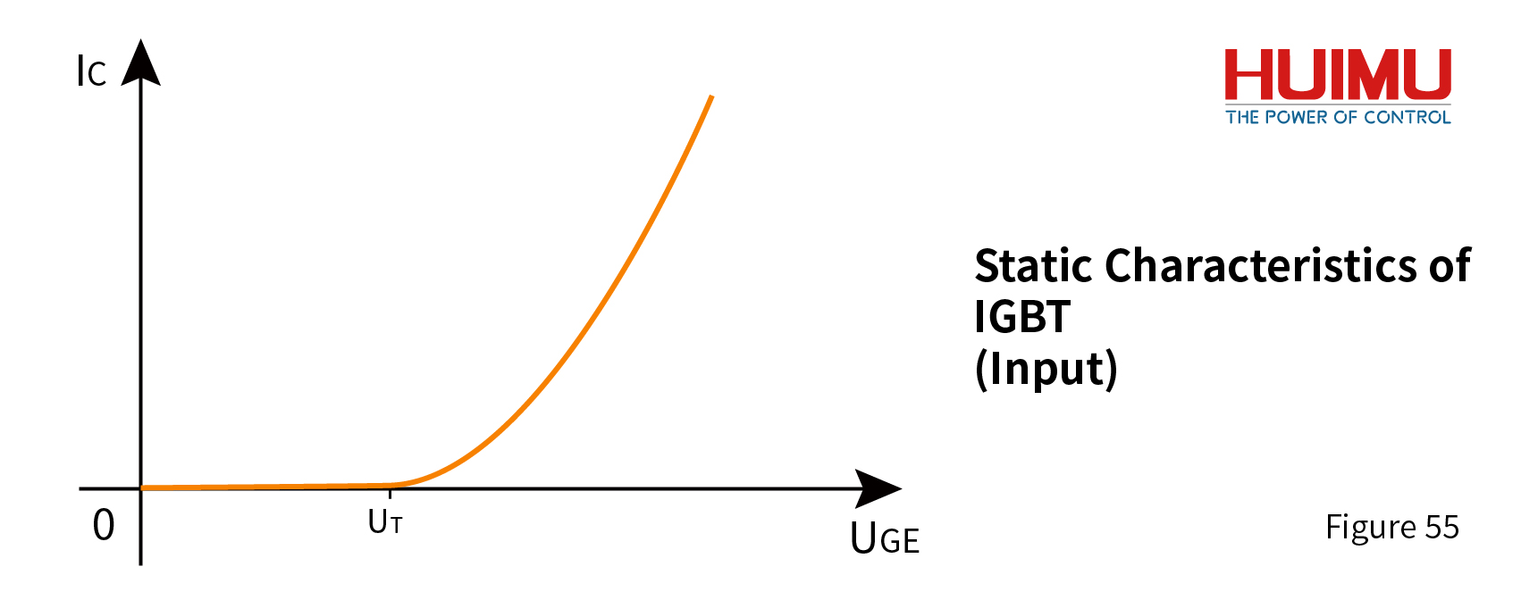
The static input characteristic curve of IGBT is similar to the static input characteristic curve of MOSFET.
2- Output Characteristics
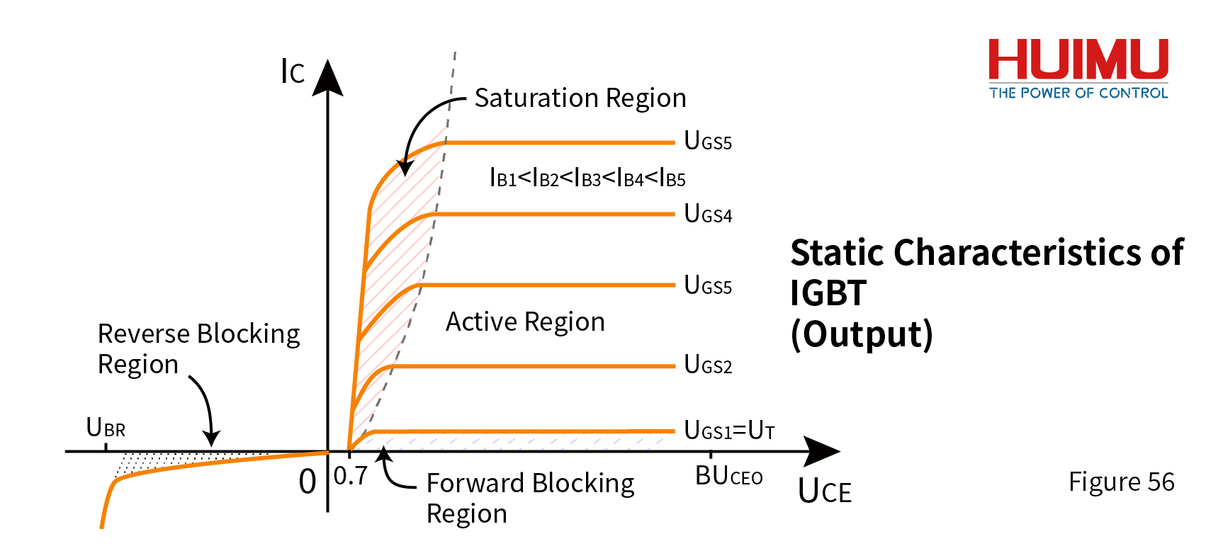
The static output characteristics of IGBT can be divided into forward blocking region, active region, saturation region, and reverse blocking region. IGBT usually only works in the switching state (that is, fast switching back and forth between the forward blocking region and the saturation region) to prevent the IGBT from being burned out due to excessive power consumption when working in the active region.
Forward Blocking Region: Similar to the cut-off region of BJT. When UGE < UT, the internal MOS channel of the IGBT is pinched off, and there is a leakage current ICEO between the collector and the emitter.
Active Region: Similar to the active region (amplification region) of BJT. When UGE ≥ UT and UCE > UGE - UT, IGBT works in the active region and will produce a 0.7V on-state voltage drop. In the active region, the electron current IN flowing into the N base region is controlled by the gate voltage UGE, which limits the base current IB1 of V1, and then the hole current IP is limited, so the collector current IC will enter a saturation state (similar to the saturation state of a MOSFET). In the active region, the voltage and current that the IGBT bears are very large, and the power consumption of the IGBT is also very large, so IGBT should cross this region as soon as possible.
Saturation Region: Similar to the saturation region of BJT. The saturation region of IGBT is also known as ohmic region or variable resistance region. When UGE ≥ UT, and UCE ≤ UGE - UT, the collector current IC is no longer controlled by the gate voltage UGE, but determined by the external circuit.
Reverse Blocking Region: Similar to the reverse blocking state of power diode.
* The Difference between MOSFET Saturation Region and IGBT Saturation Region
The saturation voltage drop after the IGBT is completely turned on mainly depends on the conductance modulation, while the turn-on voltage drop of the MOSFET mainly depends on the drain current (resistance characteristic). Therefore, the saturation region of MOSFET refers to current saturation, and the saturation region of IGBT refers to voltage saturation.
5.4.2 Dynamic Characteristics of IGBT
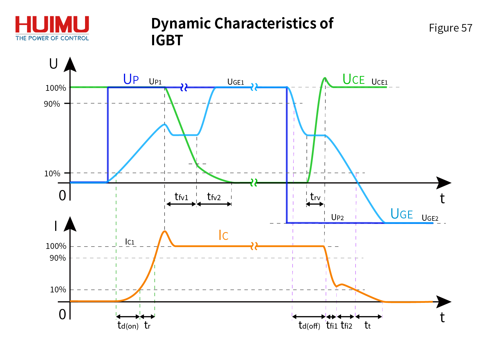
The dynamic characteristics of IGBT are similar to the combination of MOSFET and BJT.
1- Turn-on Process
The turn-on process of IGBT is similar to that of MOSFET. Generally, the time taken from UGS rising to 10% UGS1 to IC rising to 10% IC1 is called the turn-on delay time td(on). The time taken for IC to rise from 10% IC1 to 90% IC1 is called the rise time tr. The turn-on time ton of the IGBT is the sum of td(on) and tr. However, it should be noted that the falling process of UCE is divided into two stages -- the tfv1 stage is the stage when the equivalent MOSFET works alone; the tfv2 stage is the stage when the equivalent MOSFET and the equivalent BJT work together.
The calculation formula of the turn-on time: ton = td(on) + tr
2- Turn-off Process
The turn-off process of IGBT is similar to that of MOSFET and BJT. Generally, the time taken from UGS falling to 90% UGS1 to IC falling to 90% IC1 is called the turn-off delay time td(off). The time taken for IC to fall from 90% IC1 to 10% IC1 is called the fall time tf. The turn-off time toff of the MOSFET is the sum of td(off) and tf. However, it should be noted that the falling process of IC is divided into two stages -- the tfi1 stage is the stage when the equivalent MOSFET works alone; the tfi2 stage is the stage when the equivalent MOSFET and the equivalent BJT work together. The tail time tt is the time required for the reverse recovery current to disappear. Due to the holes injected into the P+ collector region are recombined in P+ collector region, so the residual current is reduced and the tf is shortened.
The calculation formula of the turn-off time: toff = td(off) + tf = td(off) + tfi1 + tfi2
5.5.4.3 Safe Operating Area of IGBT
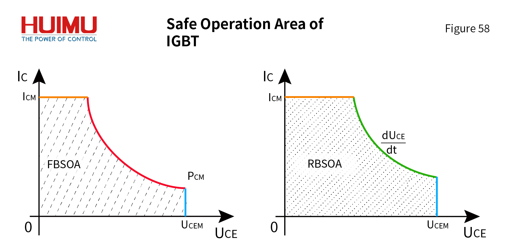
Positive-biased safe operating area (FBSOA): Determined by ICM, UCEM and PCM.
Reverse-biased safe operating area (RBSOA): Determined by ICM, UCEM and dUCE/dt.
5.5.5 Series and Parallel Connection of IGBT
Similar to MOSFET, IGBT is not suitable for series connection.
The temperature characteristic of the on-resistance RON of the IGBT is affected by the collector current IC. When IC ≤ 1/3 ICM, the on-resistance RON of IGBT has a negative temperature coefficient, which is not suitable for parallel connection. When IC > 1/3 ICM, the on-resistance RON of IGBT presents a positive temperature coefficient, which is suitable for parallel connection as the same as MOSFET. When the current is small, the impact of uneven current on the IGBT is relatively small, so overall IGBTs are still very suitable for parallel connection.
5.6 Other Fully-controlled devices
Through the composite structure, a fully-controlled device that integrates the advantages of multiple devices can be manufactured, such as MCT, SIT, SITH, IGCT, etc.
1- MOS Controlled Thyristor
The MOS controlled thyristor (MCT) combines the advantages of MOSFET and thyristor, which has the advantages of extremely high di/dt and dv/dt tolerance, fast switching speed, low on-state voltage, small switching loss, high voltage capacity, and high current capacity. Similar to GTO, the MCT is composed of tens of thousands of MCT units, and each unit is composed of a PNP thyristor and a MOSFET. The MOSFET controls the working state of the PNP thyristor. However, although the idea of MCT is similar to that of IGBT, its voltage and current capacity are far from the expected value, and the cost is higher than that of IGBT, so it cannot be put into the market.
2- Static Induction Transistor
The static induction transistor (SIT) is a kind of the junction field effect transistor with majority carriers participating in conduction process. The operating frequency of SIT is equivalent to or even higher than that of Power MOSFET, and its power capacity is larger than that of MOSFET, so it is suitable for high frequency and high power applications. SIT is a normally open (NO) switch -- when no signal is applied, the SIT is turned on; when a negative bias is applied, the SIT is turned off. In practical applications, the normally open switch is not as safe as the normally closed switch. In addition, the on-state resistance of SIT is large, and the on-state loss is also large, so SIT cannot be widely used like Power MOSFET. SIT is mainly used in the fields of radar communication equipment, ultrasonic power amplification, pulse power amplification and high-frequency induction heating.
3- Static Induction Thyristor
The static induction thyristor (SITH) is a bipolar field controlled thyristor (FCT). Many characteristics of SITH are similar to GTO. SITH has the advantages of conductance modulation effect, low on-state voltage, and large current capacity. The switching speed of SITH is much higher than that of GTO, and the current turn-off gain is smaller than of GTO. SITH has both normally open and normally closed types.
4- Integrated Gate-Commutated Thyristor
The integrated gate-commutated thyristor (IGCT, or GCT) combines the advantages of IGBT and GTO. Its power capacity is equivalent to GTO, and the switching speed is 10 times that of GTO. IGCT does not need complicated buffer circuit, but its driving power is still very large. Both IGCT and IGBT may replace GTO in the high-power field.