§7. How to use Power Electronic Devices
7.1 Introduction to Power Electronic System
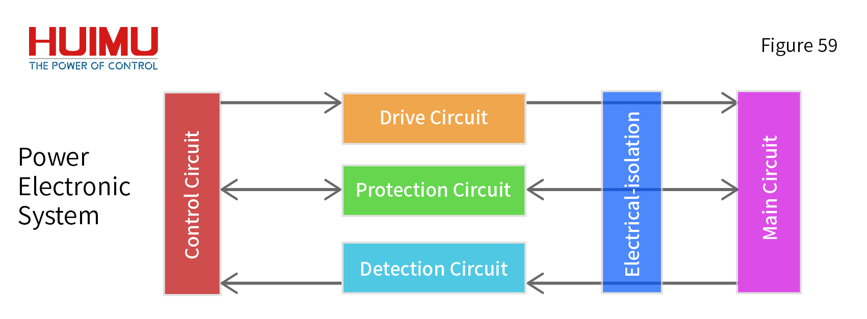
Power electronic devices cannot be used directly, and a power electronic system (PES) needs to be built first. The power electronic system is composed of a main circuit, a control circuit, a drive circuit, a detection circuit and a protection circuit.
Main Circuit: It is used to realize the change or control of electric energy. Power electronic devices are the core components of the main circuit.
Control Circuit: It is used to provide control signals to the drive circuit.
Drive Circuit: It is used to convert the control signal of the control circuit into a gate signal for the main circuit.
Detection Circuit: It is used to detect the working status of the main circuit and feed it back to the control circuit.
Protection Circuit: It is used to protect the control circuit and the main circuit to ensure the reliable operation of the entire system.
Electrical Isolation: It is used to isolate the control circuit (small current) from the main circuit (large current).
As the most common power electronic device, the internal structure of a solid state relay is a basic power electronic system (The working principle of Zero-Crossing AC Solid-State Relays).
7.2 How to drive Power Electronic Devices
The drive circuit is the interface between the main circuit and the control circuit, and is used to convert the control signal of the control circuit into a turn-on signal or a turn-off signal for the main circuit. For half-controlled devices, the drive circuit only needs to provide a turn-on signal. For fully-controlled devices, the drive circuit should provide a turn-on signal and a turn-off signal. When designing the drive circuit, many factors need to be considered to make the power electronic devices work in an ideal state. A good driving circuit can effectively decrease the switching time and switching power consumption of power electronic devices, and at the same time can ensure the working efficiency, safety and reliability of power electronic devices.
According to the type of the drive signal, the drive circuit can be divided into the current-driven circuit and the voltage-driven circuit. The current drive circuit can provide a current drive signal and a threshold voltage for the current-driven device; the voltage drive circuit can provide a voltage drive signal for the voltage-driven device. The voltage-driven circuit is easier to design and manufacture than the current-driven circuit, so the voltage-driven devices are more popular. The drive circuit can also be divided into the discrete drive circuit and the integrated drive circuit. The discrete drive circuit need to be designed separately for different power electronic devices, and also need to consider issues such as parameter matching and electromagnetic compatibility. Therefore, in order to achieve the best performance of the power electronic device, the integrated drive circuit specially developed by the device manufacturer is usually preferred.
Since the control circuit is usually formed by information electronic devices with a very low operating power, and the power of the main circuit is very large, the drive circuit also needs to provide electrical isolation between the control circuit and the main circuit to prevent the signal from the main circuit from damaging the control circuit. The isolation method can be usually divided into optical isolation and transformer isolation (magnetic isolation).
1- Optical Isolation
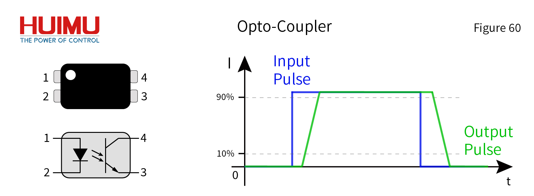
Optical isolation refers to the transmission of the control signal to the main circuit through light. Generally, a photocoupler (optocoupler, OPT) is used for optical isolation, and the light-emitting diode (LED) in the optocoupler controls the phototransistor through optical signals. The input current ID of the photocoupler is equivalent to the base current of a general transistor, and the output current IC is equivalent to the collector current of a general transistor. The input and output characteristics of optocouplers are similar to BJT. The current gain ID/IC of ordinary optocouplers is usually less than 1. The high transmission ratio type optocoupler will use Darlington structure to increase its current gain, but the withstand voltage of the optocoupler is limited (generally within 2000V). The light triggered thyristor transmits the control signal through the optical fiber, so there is no need to add additional optical isolation measures. At the same time, the light triggered thyristor is a half-controlled device, so there is no need to consider how to turn it off.
2- Transformer Isolation
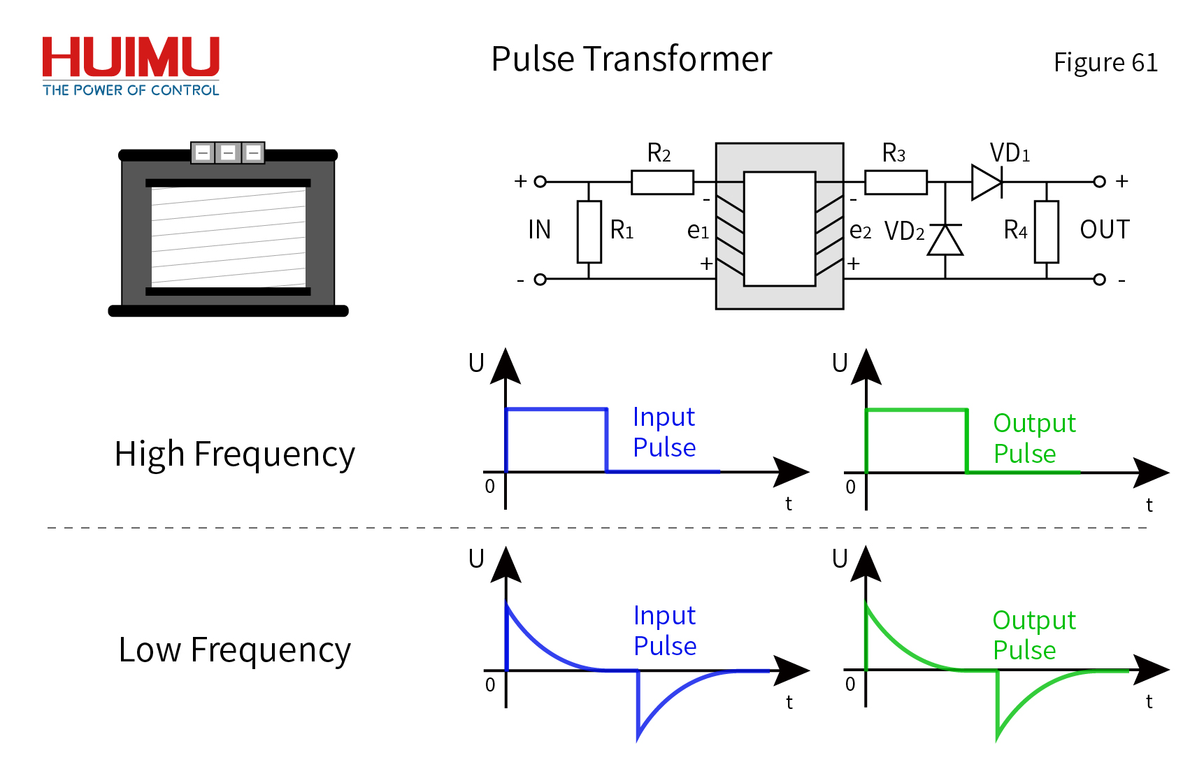
Transformer isolation refers to the isolation of the primary winding and the secondary winding through the iron core of the pulse transformer, and the use of the magnetic saturation characteristics of the iron core to transmit the control signal from the input circuit to the output circuit. Due to the non-linear distortion characteristics of transformers, pulse transformers are generally suitable for high-frequency signals, so heating and loss must also be considered. Since the pulse transformer generally works at the initial permeability of the core, the volume of the pulse transformer will be much larger than other transformers.
7.2.1 Drive Circuit of Half-controlled Device
1- Turn-on Requirements
● Ensure a certain pulse width (pulse sustain time) so that the internal positive feedback of the thyristor can be established to ensure the reliable conduction of the thyristor.
● Ensure a certain pulse flat top amplitude to provide sufficient drive current, and at the same time avoid the appearance of burrs to interfere with the normal operation of the thyristor.
● Ensure that the gate voltage, gate current and gate power are all within the rated trigger area to avoid damage to the SCR.
● Provide necessary protective measures, such as electrical isolation, temperature control, anti-interference, etc.
2- Common Drive Circuit
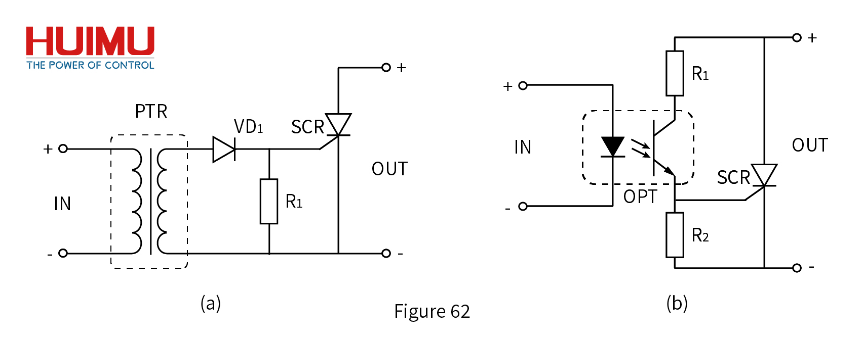
● If the load power is large, a pulse transformer (PTR) can be used as the electrical isolation device, as shown in Figure 61, a. In order to obtain a gate pulse current with a sufficiently large amplitude, a sufficiently long duration, and the shortest possible current rise time, a transistor amplifier (TRA) is usually added to the input side of the pulse transformer (PTR).
● If the load power is small, a optocoupler (OPT) can be used as an electrical isolation device, as shown in Figure 61, b.
7.2.2 Drive Circuit for Fully-control Device (Current Drive)
The parameters of fully-controlled power electronic devices are different, so their drive circuits are also different. Generally, the current drive type drive circuit is usually more complicated than the voltage drive type. It is generally recommended to directly use the integrated drive circuit provided by the manufacturer to ensure the performance of power electronic devices as much as possible.
7.2.2.1 Drive Circuit of GTO
1- Turn-on Requirements
● Same as that of thyristor.
2- Turn-off Requirements
● It is necessary to provide a turn-off current (provided by the gate reverse bias circuit) much larger than the turn-on current to speed up the turn-off process of GTO.
3- Common Drive Circuit
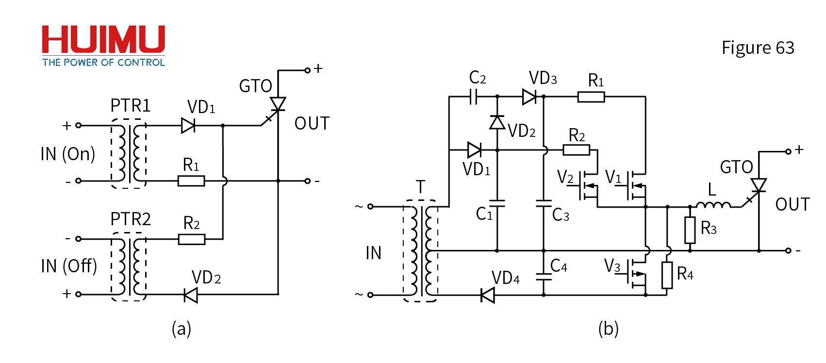
The drive circuit of GTO usually includes turn-on drive circuit, turn-off drive circuit and gate reverse bias circuit. And the drive circuit of GTO can be divided into the pulse transformer coupling type and the direct coupling type. The common discrete drive circuit of GTO is shown in Figure 62:
● Pulse transformer coupling drive circuit is shown in Figure 62, a. The pulse transformer provides electrical isolation. And the pulse signal on the secondary winding of the pulse transformer directly drives the GTO. However, the pulse transformer has leakage inductance, which will affect the switching speed of the GTO, and also lead to the inability to form a steep pulse front. The direct coupling circuit can avoid this problem.
● Direct coupling drive circuit is shown in Figure 62, b. The isolation circuit (transformer or optocoupler) provides electrical isolation; VD1 and C1 provide +5V voltage; VD2, VD3, C2, C3 form a voltage doubling rectifier circuit, providing +15V voltage; VD4 and C4, provide -15V voltage. When V1 is turned on, it outputs a strong positive pulse. When V2 is turned on, it output a flat top part of the positive pulse. When V2 is turned off and V3 is turned on, it outputs the negative pulse. When V3 is turned off, R3 and R4 provide negative gate bias voltage. The direct coupling drive circuit can avoid mutual interference and parasitic oscillation within the circuit, and can provide a relatively steep pulse front, but its design is complicated, power consumption is large, and efficiency is low. However, considering the comprehensive factors, the direct coupling drive circuit still has a wide range of applications.
7.2.2.2 Drive Circuit of GTR
1- Turn-on Requirements
● Same as that of thyristor.
2- Turn-off Requirements
● A certain negative base current needs to be applied to reduce the turn-off time and turn-off loss.
● A negative bias of a certain amplitude (about 6V) needs to be applied between the base and the emitter to make the GTR turn-off more reliable.
3- Common Drive Circuit
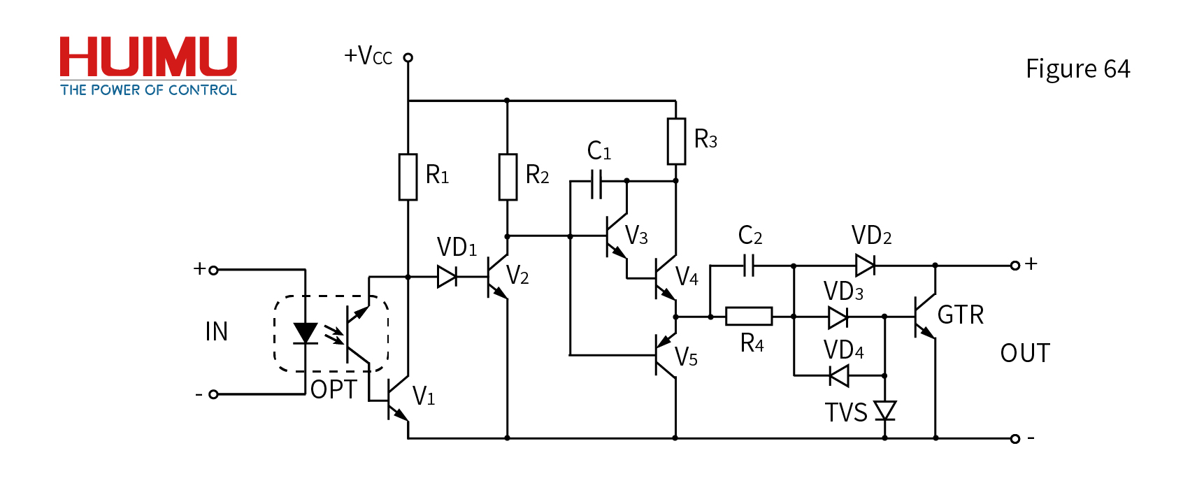
The common discrete drive circuit of GTR is shown in Figure 63. The transistor amplifier circuit is between the main circuit and the optocoupler, which is mainly composed of a transistor amplifier. The main circuit is at a low potential when it is turned on, and at a high potential when it is turned off. Therefore, the transistor amplifier circuit needs to be powered separately and electrically isolated from the main circuit power supply to avoid potential fluctuations of the main circuit from affecting the working of the amplifier circuit.
When the load is small, if all the emitter current of V4 is injected into the GTR, it will oversaturate the GTR, and its de-saturation time will be prolonged when it is turned off. Therefore, the clamp power diode VD2 and the potential compensation power diode VD3 are usually added to form a Baker clamp anti-saturation circuit. When the GTR is oversaturated, the collector potential is lower than the base potential, VD2 will automatically turn on, so that the excess drive current flows into the collector, maintaining Ubc≈0. With the help of Baker circuit, the GTR is in critical saturation when it is turned on, and it is easy to be turned off.
The accelerating capacitor C2 is used to speed up the switching process of GTR. When the GTR is turned on, R4 is short-circuited by C2, which causes the drive current to overshoot and at the same time increases the steepness of the pulse front to speed up the turn-on process. When V4 is turned on, C2 will be charged to prepare for the turn off of GTR, and its charging polarity is left positive and right negative. When V4 is off and V5 is on, the charging voltage on C2 provides a reverse voltage for the emitter junction of the GTR, so that the GTR will be quickly turned off.
The forward characteristic of the unidirectional transient voltage suppression power diode TVS is the same as that of the ordinary stabilized voltage power diode, and its reverse characteristic is a typical PN junction avalanche device. TVS has the advantages of fast response time, large transient power, low leakage current, small size, and easy to control the clamping voltage. TVS can also effectively absorb surge pulses and eliminate crosstalk. When a transient overvoltage pulse is applied to both ends of the TVS, its impedance will change from high impedance to low impedance within a few picoseconds to absorb up to several kilowatts of surge power and clamp its voltage at both ends to the preset value.
7.2.3 Drive Circuit for Fully-control Device (Voltage Drive)
1- Turn-on Requirements
● Need to provide a stable turn-on drive voltage: For MOSFET is generally 10-15V; for IGBT is generally 15-20V.
● The output resistance of the drive circuit needs to be small enough (tens to hundreds of ohms) to quickly establish the drive voltage.
● A resistor with low resistance (tens of ohms) needs to be connected in series to the gate to consume feedback energy, reduce the gain of the amplifier circuit, and reduce parasitic oscillation.
2- Turn-off Requirements
● It is necessary to apply a certain amplitude of negative driving voltage (usually 5-15V) to reduce the turn-off time and turn-off loss, and improve the reliability of the turn-off.
3- Common Drive Circuit
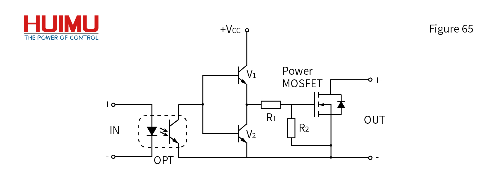
Similar to the drive circuit of GTR, the voltage drive circuit also includes an electrical isolation circuit and a transistor amplifying circuit, as shown in Figure 64. However, the voltage drive circuit only needs to provide a voltage drive signal, so its design is much simpler than that of GTR.
* Parasitic Oscillation
Parasitic oscillation refers to the oscillation that is generated by the internal parasitic parameters of the transistor amplifier, which has nothing to do with the operating frequency or is not within the operating frequency range. Parasitic oscillation can be divided into low-frequency parasitic oscillation (lower than the operating frequency) and high-frequency parasitic oscillation (higher than the operating frequency). Even if the input terminal of the transistor amplifier is short-circuited, there is usually an oscillating signal at the output terminal. But if handled properly, the parasitic oscillation can be completely eliminated. Parasitic oscillation has the following characteristics:
● The oscillation period of the parasitic oscillation is generally regular and the waveform is relatively regular.
● The amplitude of parasitic oscillation is generally large, and sometimes it can even trigger the turn-on and turn-off of power electronic devices.
● Except for low frequency oscillation caused by poor power supply decoupling, the oscillation frequency of parasitic oscillation is generally high, and the oscillation frequency and amplitude will vary with the component parameters of the transistor amplifier.
7.3 How to protect Power Electronic Devices
The protection circuit can provide a safe and reliable working environment for power electronic devices. The reasons for the damage of power electronic devices are mainly divided into overcurrent and overvoltage. In the event of overcurrent, the internal structure of power electronic devices will be destroyed due to a sharp rise in temperature. Overvoltage is usually accompanied by overcurrent, which will also cause damage to the internal structure of power electronic devices. Due to the complexity of the circuit and the consideration of safety, there is usually no single protection measure is taken, but as much protection as possible for the circuit within the cost range.
7.3.1 Overvoltage Protection
1- Overvoltage Source in Power Electronic Devices
1.1- External Overvoltage (mainly from lightning strikes and system operation process)
● Lightning Overvoltage: The overvoltage caused by lightning.
● Operating Overvoltage: During the opening and closing of the upper circuit, the overvoltage caused by the leakage inductance of the transformer in the power grid.
1.2- Internal Overvoltage (mainly comes from the switching process of power electronic devices)
● Turn-off Overvoltage: When the power electronic device is turned off, the circuit inductance induces an overvoltage at both ends of the device due to the rapid decrease of the forward current.
● Commutation Overvoltage: After the commutation of the bidirectional thyristor or anti-parallel power diode, its reverse current decreases sharply, so the line inductance will generate overvoltage at both ends of the device. Commutation means that a bidirectional device with a center symmetrical output characteristics switches back and forth between the working states of the first quadrant and the third quadrant. The commutation process inevitably accompanies the turn-on and turn-off of power electronic devices, so there must be a turn-off overvoltage during the commutation process.
2- Common Overvoltage Protection Measures
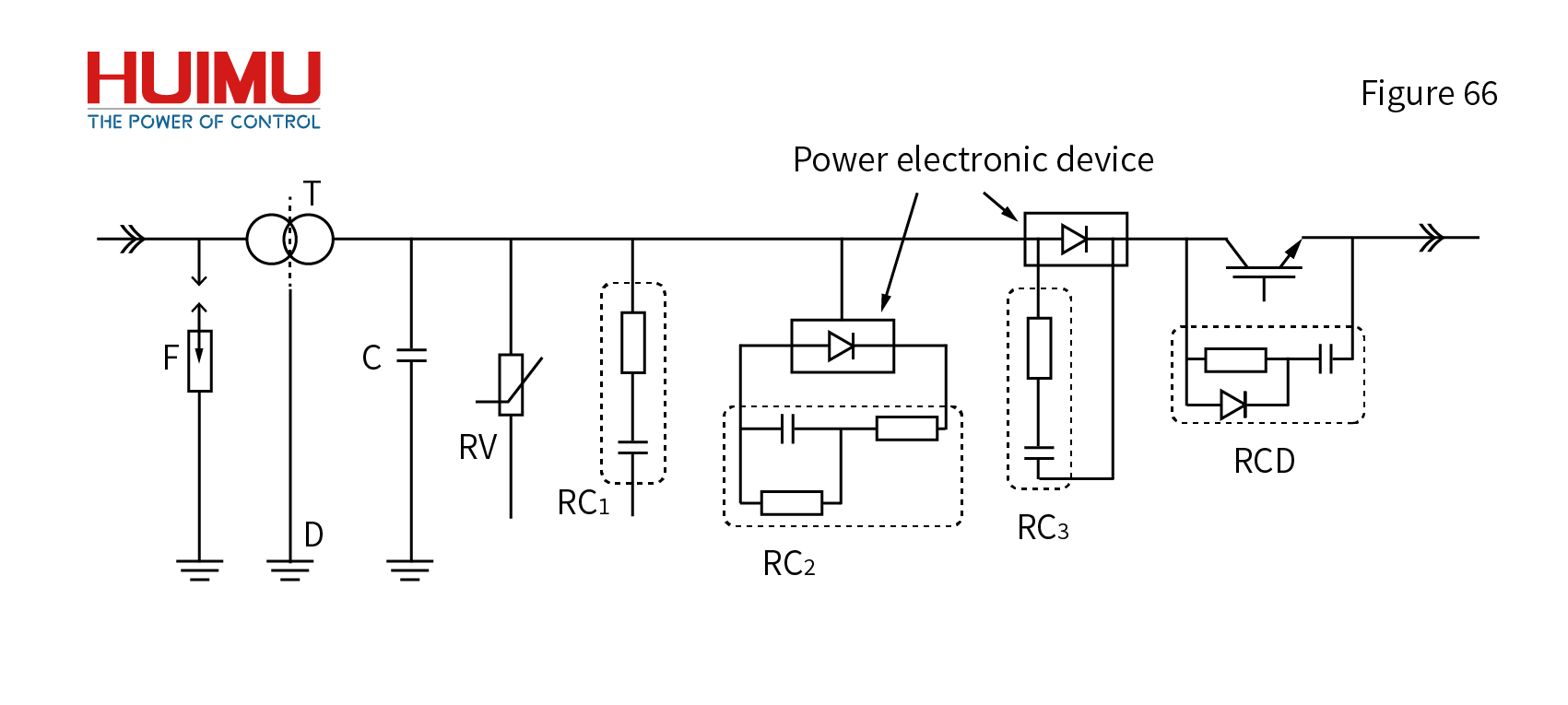
● Lightning Arrester F: It is used to conduct lightning overvoltage to the ground. The lightning arrester is generally a zinc oxide arrester, which has the same characteristics as a varistor.
● Electrostatic Shielding Layer of the Transformer D: It is used to conduct high-voltage static electricity to the ground.
● Suppression capacitor C: It is used to suppress overvoltage. However, the voltage absorbed by the capacitor will generate a larger discharge current during the discharge process.
● Varistor RV: The resistance value of the varistor decreases as the voltage increases, so It conduct the overvoltage to other circuit or the ground.
● RC1 Protection Circuit: The RC circuit adds a resistor R on the basis of the suppression capacitor C. Although its ability to absorb the overvoltage is poor, it can effectively suppress the discharge current during the discharge of the capacitor.
● RC2 Protection Circuit: The overvoltage of the external circuit will inevitably produce the DC voltage of the RC2 circuit, so the capacitor C needs to have two discharge circuits to absorb these two voltages through the resistance to leave enough margin value to deal with the next overvoltage.
● RC3 protection circuit: It is used to suppress the commutation overvoltage.
● RCD protection circuit: It is used to suppress the turn-off overvoltage.
7.3.2 Overcurrent Protection
1- Overcurrent Source in Power Electronic Devices
1.1- Overload Overcurrent: It refers to that the stable working current exceeds 120% of the rated value.
1.2- Short-circuit overcurrent: It refers to a current that has a short duration and is several times larger than the rated current.
2- Common Overvoltage Protection Measures
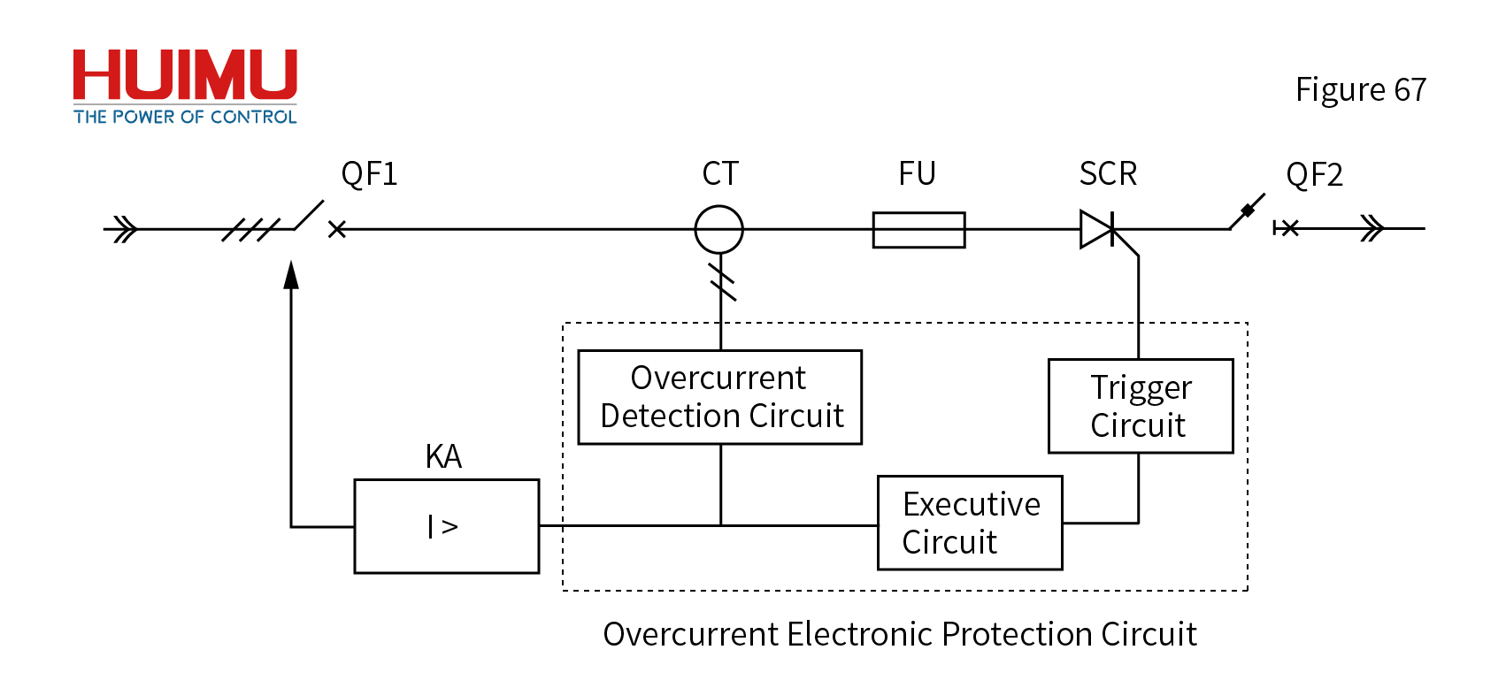
● Current Transformer CT: It is a special transformer for measurement. It consists of a closed iron core column and two mutually insulated coils sheathed on the iron core. The coil connected to the measured line is the primary side of CT. The coil connected to the detection circuit is the secondary side of CT. The primary side and the secondary side of CT are electrically isolated from each other. The main function of CT is to convert the current of the circuit under test into the current range that the detection circuit can detect. When using a current transformer, it is necessary to avoid an open circuit on the secondary side of the current transformer, because an open circuit on the secondary side will make the current transformer lose the demagnetization effect of the secondary winding. Therefore, the current of the primary winding all forms the excitation current, which increases the magnetic flux in the iron core to oversaturate the iron, which eventually leads to heat and damage to the current transformer. At the same time, if the secondary winding has a large number of turns, high voltage will be induced, which will endanger the safety of operators and equipment.
● Over-current Relay KA: When the overcurrent in the circuit is detected, the overcurrent relay starts to act, causing the AC circuit breaker QF1 to open. The action process of the overcurrent relay is relatively long, but it can directly cut off the power source of the equipment to avoid subsequent damage to the operator and the equipment.
● DC Fast Circuit Breaker QF2: The DC fast circuit breaker uses the strong short-circuit electric repulsion force to directly push the contacts open with very short action time (2-3 milliseconds), so that the short-circuit current will be shut off before reaches its maximum value. The DC fast circuit breaker is also equipped with an arc extinguishing chamber, so it has good current limiting performance.
● Fast Fuse FU: The protection methods of fast fuse can be divided into short-circuit protection and full protection (overload protection and short-circuit protection). Fast fuse is not suitable for protecting high frequency devices (such as IGBT and MOSFET). Fast fuse is usually only suitable for protecting thyristor, because the thyristor has strong current withstand capability, and both thyristor and fast fuse have second-ampere characteristics (the relationship between the overcurrent value and the maximum overcurrent withstand time). So it is easy to select the corresponding fast fuse based on the second-ampere characteristics of thyristor to ensure that the fast fuse shuts off the output circuit of the thyristor before the thyristor is damaged. Fast fuse is a disposable device, if it is blown, the fast fuse must be replaced with the same specification.
● Electronic Protection Circuit: The electronic protection circuit is mainly used to turn off the trigger circuit to make the on-state fully-controlled device switch to the high-impedance off-state, so that other power electronics devices will not be turned on and maintain the off-state. This method is invalid for the half-controlled device that has been turned on. Compared with fast fuse, the cost of electronic protection circuit is very low and the action speed is very fast, so the electronic protection circuit can effectively protect medium and high frequency power electronic devices. The electronic protection circuit is generally designed directly into the drive circuit.
7.3.3 Snubber Circuit
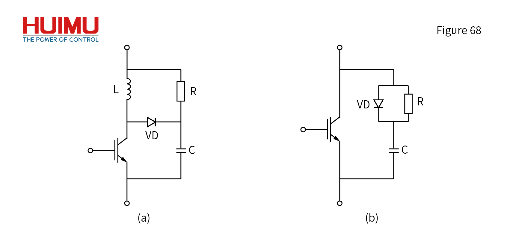
The snubber circuit (also known as the absorption circuit, or buffer circuit) suppresses the current rise rate (di/dt) of the power electronic device by using the characteristic that the inductor current cannot change suddenly, and suppresses the voltage rise rate (dv/dt) of the power electronic device by using the characteristic that the capacitor voltage cannot change suddenly. The most basic RLCD buffer circuit is shown in Figure 67, a. When the device is turned on, the inductance L suppresses di/dt; when the device is turned off, the capacitor C is charged through the fast power diode VD to absorb the overvoltage that appears on the device and limit the re-applied dv/dt. When the device is turned on, the energy on C is consumed by the resistor R. In order to reduce power loss of the device with high operating frequency and small capacity, the RLCD snubber circuit can be simplified to the RCD snubber circuit, as shown in Figure 67, b.
According to the destination of energy, the snubber circuit can be divided into an energy-consuming snubber circuit and an energy-feeding snubber circuit. The energy-consuming snubber consumes excess energy with resistors. The energy-feeding snubber circuit has no resistor, and will use the excess energy.
According to the application, the snubber circuit can be divided into turn-on snubber circuit (di/dt suppression circuit), turn-off snubber circuit (dv/dt suppression circuit) and composite snubber circuit (combination of turn-on snubber circuit and turn-off snubber circuit). The turn-on snubber circuit is used to suppress the current overshoot and di/dt to reduce the turn-on loss of the power electronic device. The turn-off snubber circuit is used to absorb the overvoltage generated by the line inductance and suppress the dv/dt to reduce the turn-off loss of the power electronic device. The current power electronic device has a high di/dt tolerance and high current tolerance, so usually there is no need to add an additional turn-on buffer circuit.
The fully controlled self-shut-off device (such as GTR and GTO) must use composite snubber circuits. The turn-on snubber circuit of GTR is used to suppress the di/dt during the turn-on process, so as to avoid overheat and second breakdown. It also plays a role in suppressing the di/dt and the peak penetration short-circuit current in the GTR inverter. The turn-off snubber circuit of GTO is not only to limit the dv/dt and overvoltage of the re-applied voltage when the GTO is turned off, but also to reduce the turn-off loss of the GTO, so that the GTO play its due turn-off capability and give full play to its load capacity. The function of the snubber circuit of IGBT focuses more on the absorption and suppression of overvoltage during the switching process. This is because the operating frequency of the IGBT is very high, so even a small circuit inductance produces a high di/dt, which leads to overvoltage and endangers the safety of the IGBT. The Power MOSFET uses a snubber circuit to suppress di/dt and dv/dt, mainly to change the switching process trajectory of the device, to reduce the switching loss, and to make the device operate reliably.
