§4. What is an Half-controlled Device?
4.1 Introduction to Half-controlled Devices
Half-controlled device (also known as thyristor, or Silicon Controlled Rectifier SCR) is a bipolar device that can be turned on but not turned off through a control signal (gate trigger). The thyristor was born in 1956 and has a very wide range of applications in the 1960s and 1970s. However, with the birth of fully-controlled devices in the 1980s, the status of thyristors was gradually replaced. However, because the thyristor can withstand very large voltages and currents, and has a simple structure and reliable operation, it still retains an important position in large-capacity applications. The thyristor has three terminals. According to its shape, the thyristor can be divided into bolt type (usually the bolt is an anode, which can be tightly connected with the radiator and easy to install) and the flat type (the flat thyristor can be clamped by two radiators). In addition to gate triggering, the thyristor will also be turned on due to the following reasons: The anode voltage rises to a very high value and causes the avalanche effect, that is, the reverse biased PN junction in the middle is broken down; the anode voltage rise rate dv/dt is too high, that is, the junction capacitance effect of the PN junction; the junction temperature is high; light triggering. On the whole, only gate triggering is the most accurate, rapid and reliable control method. However, due to the development of semiconductor technology, modular thyristors are now common (click to view more thyristor modules).
4.2 How does the Thyristor work?
4.2.1 Basic Structure of Thyristors
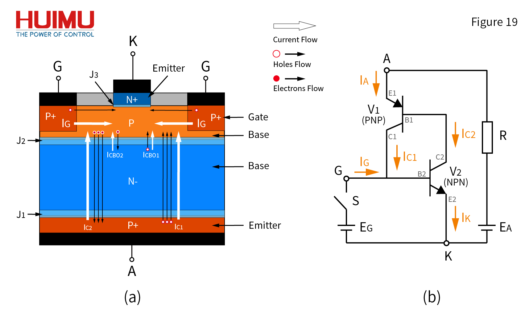
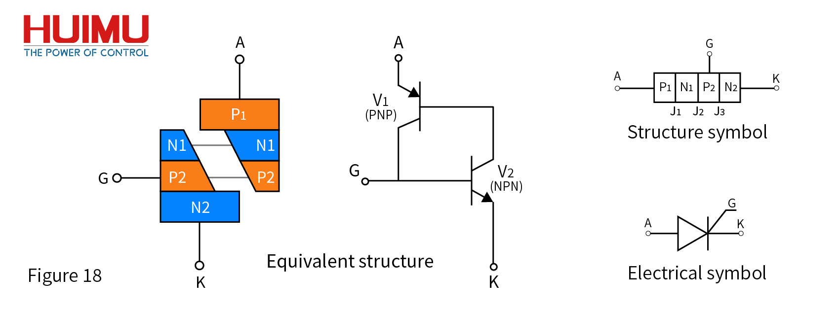
The thyristor has a P-N-P-N four-layer structure, which has one more PN junction than transistor. The thyristor has three terminals -- anode A, cathode K, and gate G. The doping degree of the P-type semiconductor and the N-type semiconductor of the thyristor are different. The internal structure of the thyristor can be equivalent to two transistors V1 and V2, as shown in Figure 19, a. V1 is a PNP transistor (P+|N-|P). P+ region is the emitter region, N- region is the base region, and P region is the collector region. V2 is an NPN transistor (N+|P|N-). N+ region is the emitter region, P region is the base region, and N- region is collector region. Similar to the transistor, when using a thyristor, be careful not to connect the cathode and anode reversely to prevent the thyristor from being burned.
4.2.2 Working Principle of Thyristors
The equivalent working circuit of the thyristor is shown in Figure 19, b. V1 and V2 are equivalent transistors. The anode and cathode of the thyristor are connected to the output circuit, and the gate of the thyristor is connected to the input circuit. EA is the power supply in the output circuit, and EG is the power supply in the input circuit. R is the output resistance. IC1 is the collector current of V1, and IC2 is the collector current of V2. The current flowing through the anode is anode current IA, the current flowing through the cathode is cathode current IK, and the current flowing through the gate is gate current IG. α1 is the common base current gain of V1, and α2 is the common base current gain of V2. The idea of turning on the thyristor is similar to that of the transistor, that is, how to make the PN junction J2 generate a larger reverse current.
Cut-off State: When a forward bias voltage UAK is applied to the cathode and anode of the thyristor, and no voltage is applied to the gate, it is equivalent to that the collector and the base of V1 and V2 are open, and the thyristor is in the off state. Due to the effect of the forward bias voltage, the depletion layer of J1 and J3 becomes narrower, and the depletion layer of J2 becomes wider, so there is a reverse saturation current ICBO in J2 -- This current consists of two parts, one is the hole current ICBO1 (the common base current of V1), and the other is the free electron current ICBO2 (the common base current of V2). These two currents will flow through J1 and J3, forming the leakage current of the thyristor, which is slightly larger than the sum of the leakage currents of the two equivalent transistors. It should be noted that in the positive blocking state, α1 + α2 is very small.
Conduction State: When a forward bias is applied to the gate of the thyristor, the P+ region injects a large number of holes into the P base region -- one part of it enters the N+ region, making J3 forward conduction, and a large number of free electrons are injected into the P base region from the N + region, and the minority carrier concentration in the P base region increases, making ICBO2 increase; the other part of it enters the N- region, making the minority carrier concentration in the N- region increase, so ICBO1 increases. Both of these leakage currents will reduce the minority carriers in the N- region and narrow the depletion layer of J1. When a sufficiently large gate forward bias is given to make the depletion layer of J1 narrow to a certain extent, the dynamic balance of J1 is broken, and a large number of holes are injected into the N- region from the P+ region, which flows into the P region in the form of a reverse current and forms the current IC1, and then flows out of the thyristor from the N+ region in the form of a forward current; similarly, the free electrons in the N+ region flow from the P region to the P+ region, and form the current IC2. It should be noted that when IC1 and IC2 are not established, the base conductivity is very small, so α1 + α2 is very small. However, when IC1 and IC2 are established, due to the conductance modulation effect, the conductivity of the base region of V1 and V2 increases, which leads to the increase of IC1 and IC2. The positive feedback between these two currents makes α1 + α2 increase rapidly and approach 1, making the on-state voltage drop sharply drops, and the anode current IA sharply rises, and finally turning on the thyristor.
* Calculation Formula of Thyristor
IC1 = α1 * IA + ICBO1, (10)
IC2 = α2 * IK + ICBO2, (11)
IK = IA + IG, (12)
IA = IC1 + IC2, (13)
IA = (α2 * IG + ICBO1 + ICBO2) /[1 - (α1 + α2) ]. (14)
It can be seen from Formula 14:
When α1+α2 approaches 0, IA will tend to leak current;
When α1+α2 approaches 1, IA will tend to infinity.
4.3 Main Parameters of Thyristors
4.3.1 Static Parameters (Voltage)
1- Forward Non-repetitive Peak Voltage UDSM / Reverse Non-repetitive Peak Voltage URSM
When the gate is open, the forward non-repetitive peak voltage UDSM (also known as the maximum off-state transient voltage) is the off-state peak voltage determined by the sharp bending point of the forward volt-ampere characteristic curve; the reverse non-repetitive peak voltage URSM (also known as the maximum reverse transient voltage) is the off-state peak voltage determined by the sharp bending point of the reverse volt-ampere characteristic curve.
2- Forward Turning Voltage UBO
The forward turning voltage UBO refers to the peak voltage that causes the thyristor to transit from the off state to the on state when a forward sin half-wave voltage is applied between the anode and the cathode of the thyristor and the gate is open at the rated junction temperature (100℃).
3- Reverse Breakdown Voltage UBR
The reverse breakdown voltage UBR refers to the peak voltage that causes the reverse leakage current of the thyristor to increase sharply when a reverse sine half-wave voltage is applied between the anode and the cathode of the thyristor at the rated junction temperature (100℃).
4- Forward Off-state Repetitive Peak Voltage UDRM / Reverse Off-state Repetitive Peak Voltage URRM
The forward off-state repetitive peak voltage UDRM (also known as the off-state repetitive peak voltage) is the forward peak voltage allowed to be repeatedly applied to the device when the gate is open and the junction temperature is rated. The repetition rate is 50 times per second, and the duration of each time is not more than 10ms. Generally, UDRM is specified as 90% of UDSM. And UDRM should be 100V smaller than UBO.
The reverse off-state repetitive peak voltage URRM (also known as the reverse repetitive peak voltage) is the reverse peak voltage allowed to be repeatedly applied to the device when the gate is open and the junction temperature is rated. The repetition rate is 50 times per second, and the duration of each time is not more than 10ms. Generally, URRM is specified as 90% of URSM. URRM voltage should be lower than UBR.
UDRM and URRM will decrease with the increase of temperature. During testing and use, the temperature should be strictly regulated. Usually, the smaller one of UDRM and URRM is taken as the rated voltage of the thyristor.
5- Gate Trigger Voltage UGT
The gate trigger voltage UGT refers to the minimum gate DC voltage required to transit the thyristor from the off state to the on state when a certain value of forward voltage is applied between the anode and the cathode of the thyristor under the specified ambient temperature. UGT is generally about 1.5V.
6- Forward Average Voltage Drop UF
The forward average voltage drop UF (also known as on-state average voltage or on-state voltage drop) refers to the average value of the voltage drop between the anode and the cathode of the thyristor when the on-state current of the thyristor is the rated current under the specified ambient temperature and standard heat dissipation conditions. UF is usually 0.4-1.2V.
7- On-State Peak Voltage UT
The on-state peak voltage UT refers to the transient peak voltage when the on-state current of the thyristor is a specified multiple of the rated current.
4.3.2 Static Parameters (Current)
1- Rated On-state Current IT
The rated on-state current IT refers to the maximum power frequency sine half-wave current value allowed to flow through the thyristor under the condition of the specified ambient temperature (40°C) and the specified cooling conditions, when the conduction angle is not less than 170°, the load is resistive, and the stable junction temperature does not exceed the rated junction temperature. The unidirectional thyristor uses the rated on-state average current IT(AV) as the rated current; the bidirectional thyristor uses the rated on-state effective current IT(RMS) as the rated current. If the current waveform is not a power frequency sine half-wave, although the thyristor is a semiconductor without the same volt-ampere characteristic curve as the resistance, a resistor with the same effective value (same heating effect) can be used as the reference to determine the rated current of the thyristor (1.5-2 times the equivalent calculation result of the resistance).
2- Off-state Leakage Current IDRM / Reverse Leakage Current IRRM
IDRM and IRRM are the corresponding leakage currents of UDRM and URRM respectively, generally less than 100μA.
3- Gate Trigger Current IGT
The gate trigger current IGT refers to the minimum gate DC current required to transit the thyristor from the off state to the on state when a certain value of forward voltage is applied between the anode and the cathode of the thyristor under the specified ambient temperature. The IGT of ordinary thyristor is generally several milliamperes; the IGT of high-sensitivity thyristors is generally several micro-amperes.
4- Holding current IH
The holding current IH is the minimum current required to keep the thyristor conducting. The IH is generally tens to hundreds of milliamperes. When the gate is triggered, even if the gate signal is removed, the thyristor is still on, and the thyristor can only be turned off by reducing the anode current. When the anode current is less than IH, the thyristor will be turned off. The higher the junction temperature, the smaller the IH, the less likely the thyristor is to be turned off.
5- Latching current IL
The latching current IL refers to the minimum current required to keep the thyristor turned on after the thyristor has just turned from the off state to the on state and the gate signal is removed. For the same thyristor, IL is generally about 2-4 times of IH.
6- Inrush Current ITSM
The inrush current ITSM refers to the non-repetitive maximum forward overload current when the junction temperature of the thyristor caused by the abnormal circuit exceeds the rated junction temperature during the half cycle of the power frequency sine wave. Normally, in a forward wave, the thyristor can withstand an overload current that is 6 times the rated current. During the life of the thyristor, if the limit of the number of surges is exceeded, the thyristor may be permanently damaged.
7- Forward Turning Current IBO
The forward turning current IBO refers to the peak current that can change the thyristor from the off state to the on state when the gate is open at the rated junction temperature (100℃).
4.3.3 Dynamic Parameters
1- Turn-on time tgt
The turn-on time tgt refers to the delay time for the thyristor to switch from the off state to the on state when enough trigger signals are applied. During the turn-on process, the output voltage UAK of the thyristor will gradually decrease to the on-state voltage drop UF, and the anode current IA will gradually increase to the rated on-state current IT.
2- Turn-off time tq
The turn-off time tq refers to the time interval from when the on-state current of the thyristor drops to zero until the thyristor begins to withstand the specified off-state voltage. The tq of an ordinary thyristor is about several hundred milliseconds. The tq is not only related to the internal structure of the tube, but also related to the temperature, dv/dt, di/dt and etc. The tq can usually be reduced by increasing the reverse voltage. If the anode voltage is reapplied during the tq, the thyristor can be turned on again, but once the tq has passed, the thyristor will be turned off no matter how to increase the anode voltage (provided that the thyristor is not broken down).
The tgt and the tq determine the operating frequency of the thyristor. For high operating frequency circuits, a thyristor with a small tq should be selected (if tq is small, tgt will be smaller). This parameter is the main difference between ordinary thyristors and fast thyristors.
3- Critical Off-state Voltage Rise Rate dv/dt
The critical off-state voltage rise rate dv/dt refers to the maximum rise rate of the applied voltage of the thyristor from off-state to on-state conversion when the gate is open at the rated junction temperature. When the junction capacitor charging current is large, if the voltage rise rate is too large, the charging current will become large enough to cause the thyristor to turn on by mistake. The dv/dt of a small current thyristor (50-100A) is generally 225V/μs, and the dv/dt of a large current thyristor (above 200A) is generally greater than 50V/μs.
4- Critical On-state Current Rise Rate di/dt
The critical on-state current rise rate di/dt refers to the maximum rise rate of the on-state current that the thyristor can withstand without damage when the gate is close at the rated junction temperature. The thyristor will produce a large power loss at the moment of turning on, and due to the limited conduction expansion speed, this loss is always concentrated in the cathode region near the gate. If the current rises too fast, even if the conducting current is not large, it will easily cause the thyristor to overheat locally, causing permanent damage to the gate, and causing the thyristor to be burned out. The larger the rated current of the thyristor, the more prominent this problem.
4.4 Basic Characteristics of Thyristors
4.4.1 Static Characteristics of Thyristors
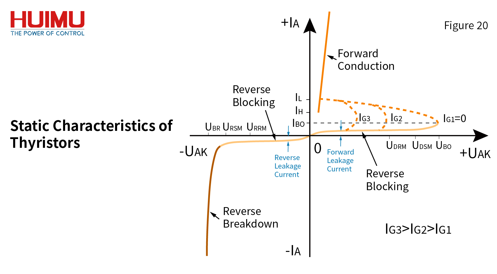
The static characteristics of the thyristor are the volt-ampere characteristics of the output current and output voltage, as shown in Figure 20. UAK is the voltage applied to the anode and the cathode of the thyristor, IA is the anode current, and IG is the trigger current.
1- Forward static characteristics
Forward Blocking State: When IG = 0, even if UAK> 0, there is only a small forward leakage current. α1 + α2 is also very small. At this time, the thyristor is in the forward blocking state. But when UAK ≥ UBO or IA ≥ IBO, α1 + α2 approaches 1, and the thyristor will enter the forward conduction state.
Forward Conduction State: The common forward conduction situation is that under the condition of IG> 0, when UAK ≥ UGT, the conductivity of the thyristor base area increases significantly, α1 + α2 approaches 1, the current IA flowing through the thyristor will approach infinity (the actual value of IA is determined by the external circuit), and finally saturated conduction is achieved. Under the same external conditions, the larger IG, the smaller UGT. It should be noted that once the thyristor is turned on, the gate loses its control function. Only when the output current IA of the thyristor is reduced to a certain value close to 0 can the thyristor be turned off.
2- Reverse Static Characteristics
The reverse static characteristics of thyristors are similar to the reverse static characteristics of power diodes. When the thyristor is subjected to a reverse voltage, no matter whether the gate has a trigger current or not, the thyristor will not be turned on, and there is only a very small reverse leakage current. At this time, the thyristor is in a reverse blocking state. However, when the reverse voltage reaches the reverse breakdown voltage UBR, it will cause the thyristor avalanche breakdown.
4.4.2 Dynamic Characteristics of Thyristors
1- Turn-on Process
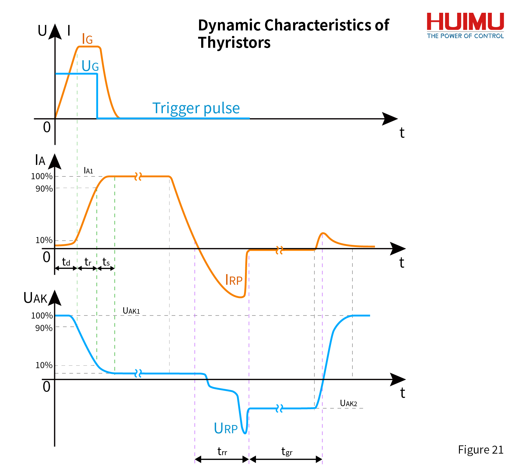
When UAK1 is applied to the output terminal of the thyristor, the thyristor is in the off state at this time, and UAK is 100% UAK1. When UG ≥ UGT, it will take a period of time before the thyristor enters the conducting state. When the thyristor is turned on, its output terminal voltage UAK will maintain a very small value, that is, the on-state voltage drop.
The turn-on process of the thyristor is divided into the delay time td, the rise time tr, and the diffusion time ts.
The delay time td is the time required for IA to rise from the forward leakage current to 10% IA1, and UAK to decrease from 100% UAK1 to 90% UAK1. The delay time is generally 0.5-1.5μs. The delay time decreases as the gate current increases.
The rise time tr is the time required for IA to rise from 10% IA1 to 90% IA1, and UAK to fall from 90% UAK1 to 10% UAK1. The rise time is affected by the characteristics of the thyristor itself, the impedance of the external circuit, the temperature, the anode voltage and etc. The rise time is generally 0.5-3μs. By increasing IA, the delay time td and the rise time tr can be significantly shortened.
The diffusion time ts is the time required for IA to rise from 90% IA1 to 100% IA1, and UAK to drop from 10% UAK1 to the on-state voltage drop. The diffusion time depends on the cross-sectional area of the cathode.
Normally, when IA reaches 90% IA1, it can be considered that the thyristor has been turned on. Therefore, the formula for calculating the turn-on time is: tgt = td + tr.
2- Turn-off Process
By reducing UAK to 0 or applying a sufficiently large reverse voltage UAK2, IA is gradually reduced, and the thyristor is converted from the on state to the off state. The turn-off process of the thyristor is divided into the reverse blocking recovery time trr, and the forward blocking recovery time tgr.
During the turn-off process, due to the inductance of the external circuit, a reverse recovery current IR appears in the thyristor. When the IR gradually reaches the peak value IRP, a corresponding URP will be generated, and then the IR will rapidly decay. The time from IA falling to zero to IR falling to the reverse leakage current of the thyristor is called the reverse blocking recovery time trr.
The time from the end of the reverse recovery process to the complete recovery of the forward blocking capability of the thyristor is called the forward blocking recovery time tgr (or gate recovery time). During the tgr, because a small number of carriers are left on the PN junction near the gate, they can still trigger the positive feedback mechanism inside the thyristor. If a forward voltage is applied to the thyristor, the thyristor will conduct forward again. No gate trigger signal is required during this turn-on process.
The calculation formula of the turn-off time tq is: tq = trr + tgr.
4.5 Series and Parallel Connection of Thyristors
1- Series Connection of Thyristors
By connecting multiple thyristors in series, the overall voltage capacity can be increased. In fact, it is not possible to multiply the withstand voltage value of a thyristor by the number to obtain the overall withstand voltage value. Instead, it should be added by the voltage actually borne by each thyristor. This is mainly because the voltage distributed on each thyristor is not uniform (divided into static uneven voltage and dynamic uneven voltage).
Static Uneven Voltage: Although the leakage current flowing through the series-connected thyristors is the same, because of their dispersion of static volt-ampere characteristics, the voltages assigned to each thyristor are not the same. In extreme cases, a certain thyristor may withstand all voltages, while other thyristors may only withstand very small voltages. The static uneven voltage can be reduced by selecting thyristors with very similar parameters and characteristics. The resistance equalization method can also be used to reduce static unevenness, that is, the thyristor is regarded as a high-resistance resistor (about 1 megohm), and each thyristor is connected in parallel with a low-resistance resistor to adjust the equivalence resistor of each parallel circuit. when their equivalent resistance values are very close, then the voltage distributed on each thyristor will also be very close.
Dynamic Uneven Voltage: The dynamic uneven voltage is caused by the difference in dynamic parameters and dynamic characteristics of the thyristor. By selecting thyristors whose dynamic parameters and characteristics are as consistent as possible, the dynamic uneven voltage can be reduced. It can also be triggered by a strong gate pulse to significantly reduce the difference in the turn-on time of the thyristor. It is also possible to use RC parallel branches for dynamic voltage equalization, that is, to absorb the over-voltage through the RC circuit, so that the voltage that each thyristor bears under dynamic conditions is very close.
2- Parallel Connection of Thyristors
By connecting multiple thyristors in parallel, the overall current capacity can be increased. Because of the different parameters and characteristics of each thyristor, it is also necessary to consider their uneven current distribution. By selecting thyristors with consistent characteristics and parameters as much as possible to reduce the dynamic uneven current and the static uneven current. It is also possible to reduce the dynamic uneven current by the current-sharing reactor (its loss is less than resistance). It is also possible to use strong gate pulse triggering to significantly reduce the difference in the turn-on time of the thyristors, so that each thyristor can be effectively triggered in a short time to achieve the purpose of dynamic current sharing. However, because the current capacity of the thyristor is getting larger and larger, it is usually unnecessary to operate the thyristor in parallel.
3- Series and Parallel Connection of Thyristors
When thyristors need to be connected in series and in parallel at the same time, it is usually recommended to connect in series firstly and in parallel secondly to ensure that the parameters and characteristics of each thyristor are as consistent as possible.
4.6 Main Types of Thyristors
1- Fast Switching Thyristor
The fast switching thyristor (FST) has excellent dynamic characteristics. Compared with ordinary thyristors, the FST has the advantages of short the turn-on time (generally 4-8μs), short turn-off time (generally 10-60μs), and large tolerance of dv/dt and di/dt. Ordinary thyristors can only work at a voltage of 50 Hz, while FST can work in circuits with higher frequencies (above 400 Hz). High-frequency thyristors (HFT) have shorter switching times and faster switching speeds than FST, and are suitable for working in high-frequency circuits (above 10kHz). Due to the high operating frequency, the heating effect of the switching loss of FST and HFT cannot be ignored, so their rated voltage and rated current are usually not high,
2- Bidirectional Triode Thyristor
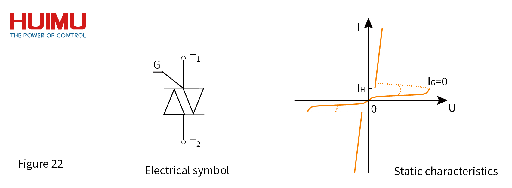
The bidirectional thyristor (also known as bidirectional triode thyristor, triode AC switch, TRIAC) can be considered as a pair of anti-parallel connected unidirectional thyristors (SCR). The bidirectional thyristor is a common core device in AC solid-state relays and modules (click to view more AC solid-state relays). The forward characteristic of the bidirectional thyristor is the same as that of the unidirectional thyristor, but its reverse characteristic is different from that of the unidirectional thyristor. The bidirectional thyristor does not have the reverse blocking ability. It can be clearly seen on the coordinate axis that the characteristic curve of the bidirectional thyristor is centrally symmetric. The bidirectional thyristor has a T1 pole (the main electrode connected to the P-type semiconductor material), a T2 pole (the main electrode connected to the N-type semiconductor material), and a gate G pole. The rated current of the bidirectional thyristor is the rated on-state effective current IT(RMS). There is no forward peak voltage and reverse peak voltage in the parameters of the bidirectional thyristor, but only the maximum peak voltage. The other parameters of the bidirectional thyristor are the same as the unidirectional thyristor.
3- Reverse Conducting Thyristor
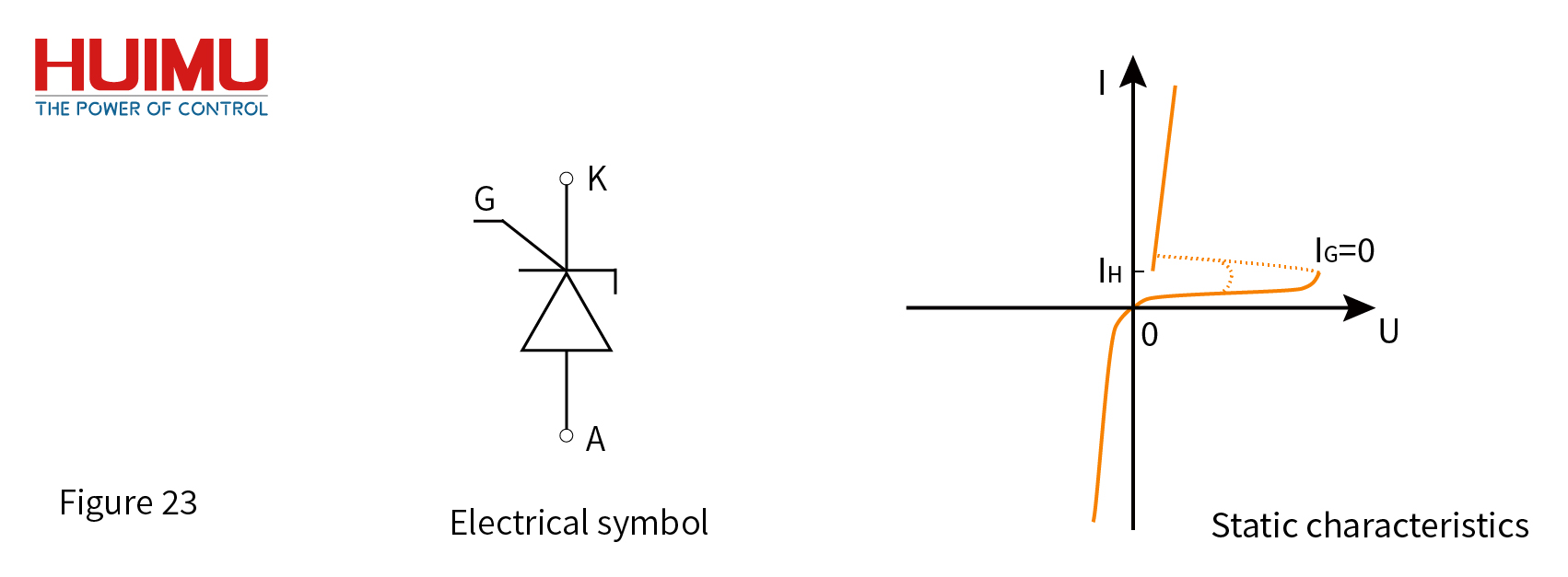
The design idea of the reverse conducting thyristor (RCT) is similar to that of the bidirectional thyristor, but the reverse conducting thyristor uses a power diode for anti-parallel connection, so that the emitter junction of the anode and the cathode are both in the short-circuit state. Due to this special structure, the reverse conducting thyristor has the advantages of low on-state voltage, short turn-off time, high rated junction temperature, high voltage resistance, high temperature resistance, and etc. For example, the turn-off time (several microseconds) and power frequency (tens of kHz) of the reverse conducting thyristor are obviously better than that of the fast switch thyristor. Reverse conducting thyristor can be regarded as an organic combination of thyristor and freewheeling power diode, which can simplify circuit design, and is widely used in applications such as switching power supplies and UPS.
4- Light Triggered Thyristor
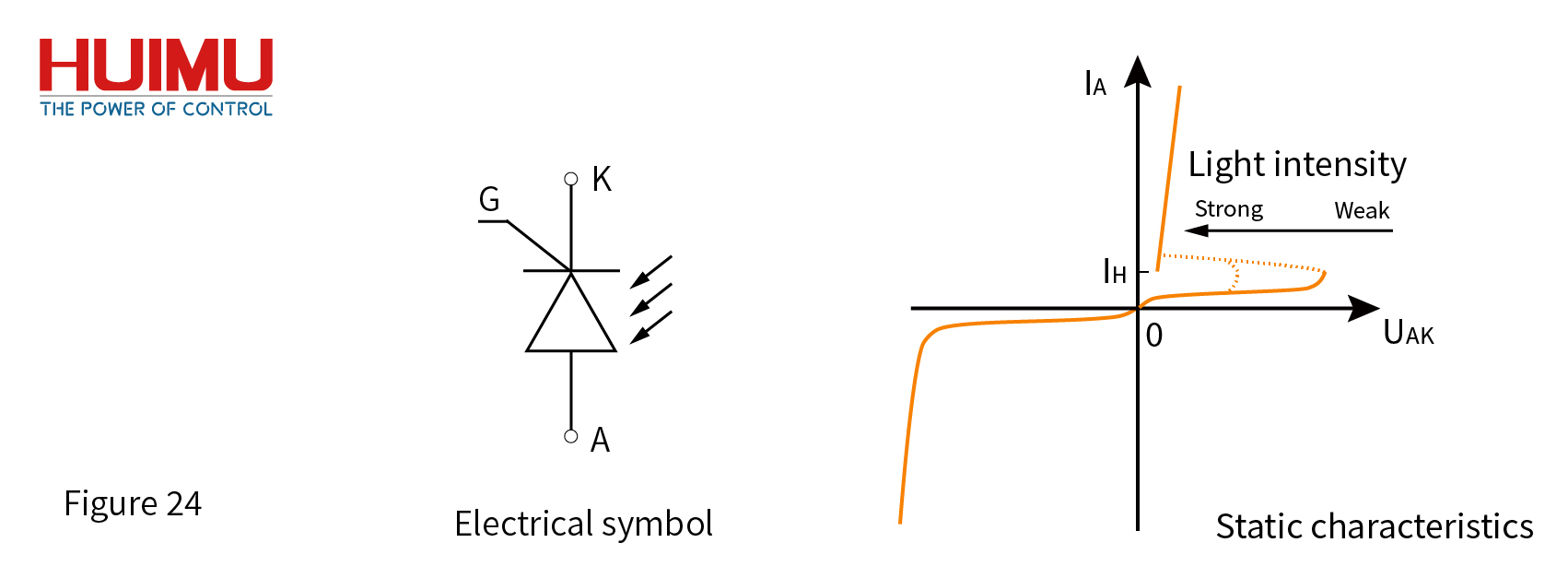
The light-triggered thyristor (also known as LTT, or light-controlled thyristor) is a thyristor that its gate region integrates a photoelectric power diode, and uses the strength of the light signal to replace the gate trigger current. Therefore, the light trigger is a kind of gate trigger. In order to improve the trigger sensitivity of the light-controlled thyristor, the gate region often adopts an amplified gate structure or a double-amplified gate structure. The light trigger ensures the electrical insulation between the main circuit and the control circuit, and can avoid the influence of electromagnetic interference. Low-power light-controlled thyristors are often used in electrical isolation to provide trigger signals for high-power thyristors. High-power light-controlled thyristors can ensure good insulation between the control circuit and the main circuit and are used in high-voltage power equipment (such as high-voltage direct current transmission).
