§3. What is a Transistor?
Before introducing half-controlled devices and full-controlled devices, it is necessary to briefly introduce bipolar junction transistors (BJT).
3.1 Introduction to Transistors
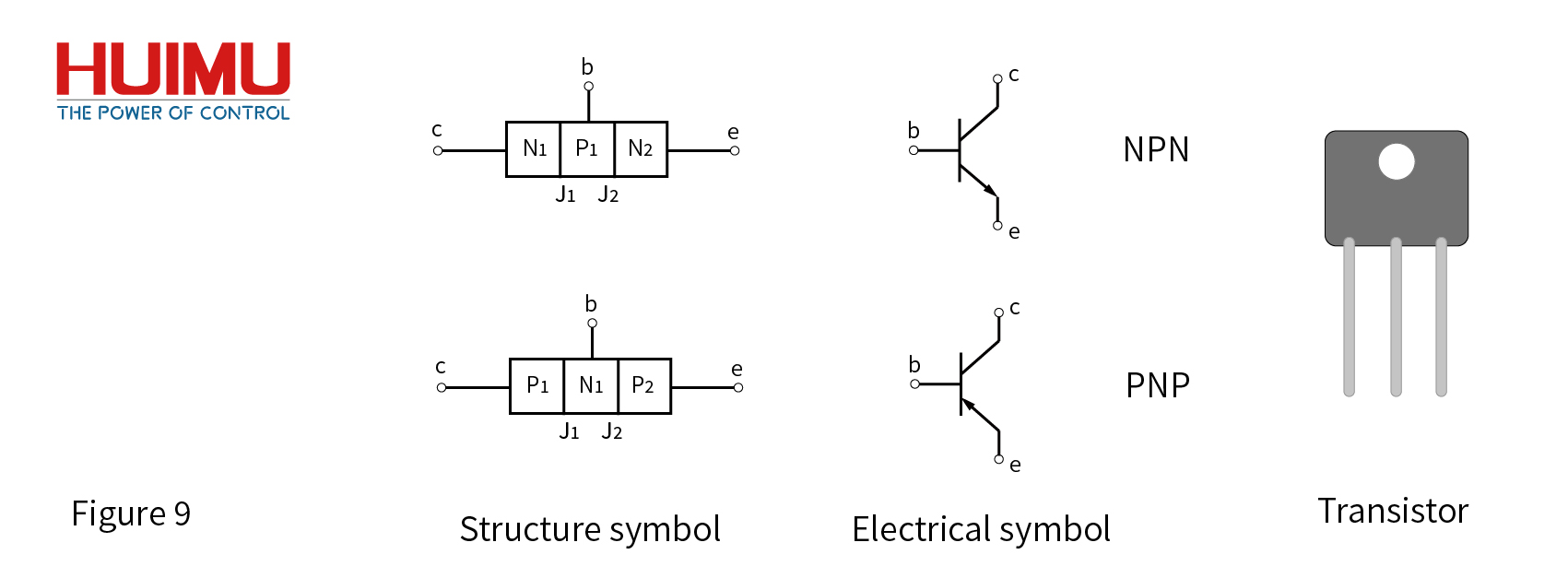
The transistor (also known as semiconductor transistor or Bipolar Junction Transistor, BJT) is a bipolar device with three terminals and two PN junctions. The transistor is one of the basic components of semiconductor devices and also one of the core components. Since its birth in the 1940s, the transistor has completely changed the structure of electronic circuits, triggered a solid-state revolution, and promoted the emergence of integrated circuits and large-scale integrated circuits. The transistor has a current amplifying function, and can control a large change in collector current with a very small change in base current, so it is often used as a contact-less switch in electronic circuits. The switching frequency of the transistor is high, and there is no mechanical service life, so it has a significant advantage over electromagnetic relays and mechanical switches.
3.2 How does Transistor work?
3.2.1 Basic Structure of Transistors
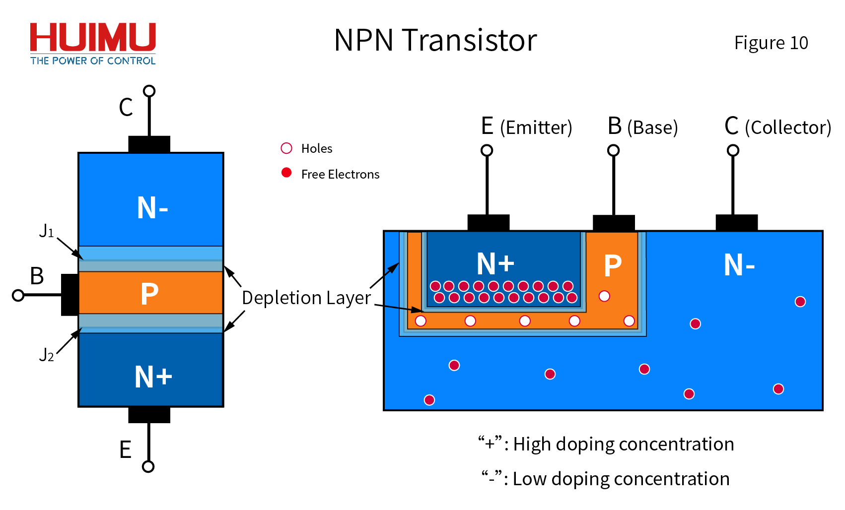
The transistor is a three-layer semiconductor structure, which has one more PN junction than Power Diode. These two closely spaced PN junctions divide the transistor into three parts with different areas and doping concentrations -- the base region is very thin (3-30μm) and the doping concentration is low; the area of emitter region is small and the doping concentration is high; the area of collector region is large and the doping concentration is low. The PN junction between the collector region and the base region is called the collector junction J1. The PN junction between the emitter region and the base region is called the emitter junction J2.
According to the material, transistors can be divided into silicon transistors and germanium transistors. According to the doping composition, transistors can be divided into PNP transistors and NPN transistors -- under forward bias, the emitter region of PNP transistors emits holes, and its direction is the same as the direction of current, so the arrow in the electrical symbol goes from the emitter to the base; under forward bias, the emitter of the NPN transistors emits free electrons, and its direction is opposite to the direction of the current, so the arrow in the electrical symbol goes from the base to the emitter.
3.2.2 Working Principle of Transistors
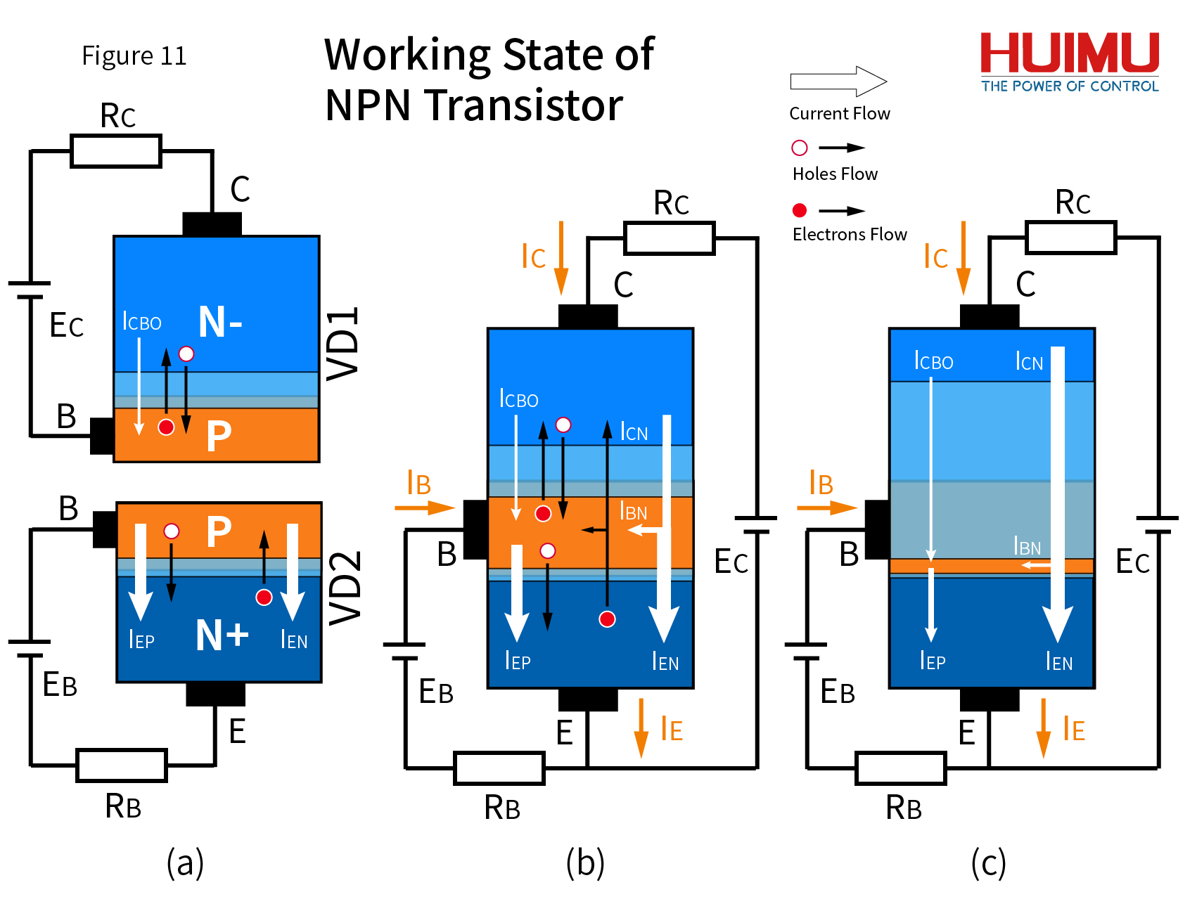
Take the NPN transistor as an example. The NPN transistor can be regarded as two equivalent diodes (VD1 and VD2), as shown in Figure 11, a. Because the N- region of VD1 has low a doping concentration and a large area, it is not prone to avalanche breakdown, so it can withstand a large reverse voltage. But in forward bias, the forward current of VD1 is very small, so VD1 is very suitable for working in reverse cut-off state. VD1 will produce a reverse saturation current ICBO when VD1 works in the reverse state, but the doping concentration of N- region and P region is very low, so the ICBO is very small. Because the N+ region of VD2 has a high doping concentration and a small area, it is prone to avalanche breakdown, so its reverse withstand voltage capability is very poor. But in forward bias, VD1 can generate a very large forward current, so VD2 is very suitable for working in the forward conduction state. When VD2 works in the forward state, it will generate two currents, one is the current IEP generated by the holes flow of the P region, and the other is the current IEN generated by the electrons flow of the N+ region. Since the doping concentration of the P region of VD1 is lower than that of the N+ region, IEN is greater than IEP. When we know the working principle of these two equivalent diodes, it is easy to understand the working principle of the NPN transistor.
Connect the NPN transistor through the common emitter connection method -- a collector power supply EC and collector resistance RC are connected in series to the collector and the emitter; a base power supply EB and a base resistance RB are connected in series to the base and the emitter. In this circuit, current flows into the NPN transistor from the collector and base, and flows out of the NPN transistor from the emitter -- the total current flowing in from the collector is the collector current IC; the total current flowing in from the base is the base current IB; the total current flowing out from the emitter is the emitter current IE. The linear relationship between IC and IE is common base current gain α, and the linear relationship between IC and IB is common emitter current gain β. It is worth noting that due to the difference in doping concentration, the collector junction J1 is not suitable for forward bias, and the emitter junction J2 is not suitable for reverse bias. If the collector and emitter are reversely connected, the possibility of NPN transistor breakdown will increase significantly.
Cut-off State: The structure of NPN makes there is always a PN junction in a reverse bias state. When no voltage is applied to the base, even if a large voltage (less than breakdown voltage BVCEO) is applied to the collector and the emitter, the NPN transistor cannot be turned on (but there is a small leakage current ICEO).
Active State: VD1 and VD2 must work at the same time to turn on the NPN transistor, so a certain voltage needs to be applied to the base to make J1 reverse biased (UBC<0) and J2 forward biased (UBE> UTO). When the NPN transistor is turned on, its internal current is a bit different from when the equivalent diodes worked separately, as shown in Figure 11, b. The free electrons injected from the N+ region into the P region do not completely recombine with the holes in the P region. Due to the reverse bias of J2, a part of the free electrons will pass through the P region and be directly injected into the N- region, and generate a reverse current ICN. When the NPN transistor is working in an active state, a small change in the base current IB of will cause a large change in the collector current IC. This phenomenon is called conductance modulation effect. This phenomenon is like a tiny input current being amplified into a huge output current, so the active state is also known as the amplification state.
Saturation State: With the increase of IB, the concentration of holes in the P region decreases, IEP decreases, and the depletion region of J1 keeps increasing. At the same time, since the free electrons injected from the N+ region into the P region are getting less and less, IBN has dropped to near the minimum value, and the amplification effect of IB on IC has begun to weaken. When IB and IC no longer have a linear relationship, the NPN transistor begins to enter a saturated state. At this time, as IB increases, IC slowly increases, and the saturation depth of the NPN transistor also begins to deepen. When almost all the free electrons in the N+ region are injected into the N- region, the base potential is the same as the collector potential (UBC=0). At this time, the NPN transistor is in a deep saturation state, and IC is completely unaffected by IB. It should be noted that as the depletion region of J1 increases, the possibility of avalanche breakdown on J1 also increases.
* Calculation Formula of Transistor
IC = ICN + ICBO, (1)
IB = IBN + IEP - ICBO, (2)
IE = IC + IB = ICN + IBN + IEP, (3)
because IC > 0, then we get IE / IC = IB / IC + 1; (4)
α = ICN / IE = (IC - ICBO) / IE, (5)
β = ICN / (IB + ICBO) = (IC - ICBO) / (IB + ICBO), (6)
because IC > IB >> ICEO >> ICBO ≈ 0, if ignoring all the leakage current, we can get α ≈ IC / IE, β ≈ IC / IB, (7)
then we can get 1/α = 1/β + 1, (8)
so the relation between α and β is: α = β / (1 + β), β = α / (1 - α). (9)
* Leakage Current
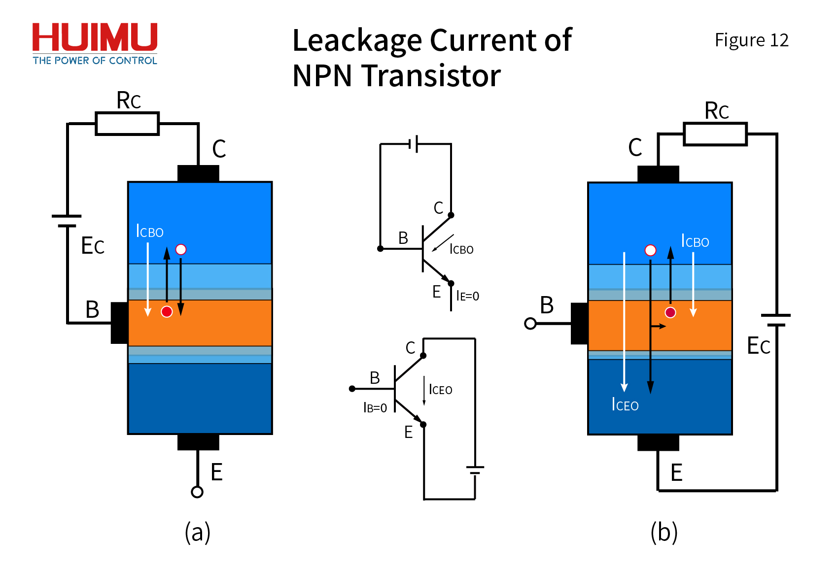
Both the collector junction reverse saturation current ICBO and the penetration current ICEO are unavoidable leakage currents in the transistor. By opening the emitter of the transistor (IE=0) and applying voltage to the collector and the base, the value of ICBO can be measured, as shown in Figure 12, a. By opening the base of the transistor (IB=0) and applying voltage to the collector and the emitter, the value of ICEO can be measured, as shown in Figure 12, b.
The generation mechanism of the collector junction reverse saturation current ICBO is shown in Figure 11, a.
The generation mechanism of the penetration current ICEO is as follows: Under the action of an external electric field, the majority carriers in the collector region move away from the PN junction, widening the space charge region, and the built-in electric field of the collector junction J1 is enhanced, which is conducive to drift motion; the majority carriers in the emitter region move closer to the PN junction, narrowing the space charge region, and the built-in electric field of the emitter junction J2 is weakened, which is not conducive to drift motion. Therefore, under the action of the built-in electric field, the minority carriers in the base region drift to the collector region through J1. At the same time, the minority carriers in the collector region drift to the base region through J1, part of which participates in the recombination of the base region, and the other part diffuses to the emitter region through J2. Due to the low doping concentration of the base region, the proportion of minority carriers participating in the recombination of the base region is very low. It is not difficult to find that this process is very similar to the generation mechanism of IEN when the transistor is turned on. Therefore, there is a linear relationship between ICEO and ICBO, ICEO = (1 + β) * ICBO. However, due to the low doping concentration of the collector region and the base region, the value of ICEO is very low and can usually be ignored. The ICEO of silicon transistors is generally less than 100nA; the ICEO of germanium transistors is generally less than 100μA.
* Conductance Modulation Effect
Conductance (G) is the reciprocal of resistance, and the unit is Siemens (S). Conductance modulation effect (also known as the base region conductivity modulation effect, or Webster effect) is one of the basic characteristics of bipolar transistors (BPT), which refers to the phenomenon that the conductivity of the base region increases significantly (or the resistivity of the base region decreases significantly) when the working current of the bipolar transistor is large. Except BJT, other bipolar transistors such as SCR, GTO, GTR and parasitic transistors in IGBT all have conductivity modulation effect. In addition to the Webster effect, when the working current of the bipolar transistor is large, the Early effect (the phenomenon that the changes of the collector junction voltage will lead to the changes of the width of the base region) and the Kirk effect (the phenomenon that the width of the base region increases) will also appear.
3.3 Main Parameters of Transistors
1- Common Base Current Gain α
Common base current gain α (the full name is "hybrid parameter forward current gain, common base", HFB), which is determined by the emitter efficiency factor and the base region transport factor, α = FE * FB. When the base is zero-biased (UBC = 0), the base short-circuit amplification factor α0 is determined by the emitter efficiency factor, the base region transport factor, the collector efficiency factor and the avalanche multiplication factor, α0 = FE * FB * FC * M.
The emitter efficiency factor FE is the ratio of the electron current IEN injected into the base region to the emitter current IE, FE = IEN / IE = IEN / (IEN + IEP) = 1 / [1 + (IEP / IEN) ]. By reducing the doping concentration of the base region, the total amount of impurities in the base region is much smaller than the total amount of impurities in the emitter region, which can effectively increase the number of minority carriers injected into the base region from the emitter region. The closer the ratio of IEP to IEN is to 0, the higher the emission efficiency of the transistor.
The base region transport factor FB is the ratio of the electron current ICN that reaches the collector region to the electron current IEN injected into the base region, FB = ICN / IEN. By reducing the width of the base region, the time that carriers from the emitter region stay in the base region can be effectively shortened, thereby increasing the number of minority carriers that transit the base region. The smaller the width of the base region, the smaller the recombination loss of electrons from the emitter region in the base region.
The collector efficiency factor FC is the ratio of the collector current IC to the electron current ICN that reaches the collector region, FC=IC/ICN.
The avalanche multiplication factor M is used to describe the avalanche multiplication effect when the reverse voltage of the collector junction increases to close to the avalanche breakdown voltage. It is usually estimated with the following formula, M = 1 / [1 - (V / VB) ^n], n is determined by the material of the PN junction (silicon: n=1.5-4; germanium: n=2.5- 8); VB is the reverse breakdown voltage of the collector J1; V is the voltage across the collector junction. When the absolute value of V tends to the absolute value of VB, M tends to infinity, and avalanche breakdown will occur in the PN junction.
Generally, hFB(α) is used to express the common base DC current gain, hFB(α) = IC / IE, and its range is usually 0.95-0.99; hfb(α) is used to express the common base AC current gain, hfb(α) = ΔIC / ΔIE. In general, hfb(α) ≈ hFB(α).
2- Common Emitter Current Gain β
Common emitter current gain β (the full name is "hybrid parameter forward current gain, common emitter", HFE) is the ratio of collector current to base current, and its value is usually much larger than 1. Generally, hFE(β) is used to express the common emitter DC current gain, hFE(β) = IC / IB, which can be measured directly by a multimeter; hfe(β) is used to express the common emitter AC current gain, hfe(β) = ΔIC / ΔIB. The current amplification factor (or forward current gain) of the transistor usually refers to the common emitter current gain β.
3- Common Collector Current Gain γ
Common collector current gain γ (the full name is "hybrid parameter forward current gain, common collector", HFC) is the ratio of emitter current to base current. Generally, hFE(γ) is used to express the common collector DC current gain, hFC(γ) = IE / IB; hfc(γ) is used to express the common collector AC current gain, hfc(γ) = ΔIE / ΔIB. This parameter is rarely used in normal times.
4- Threshold Voltage UTO
The threshold voltage UTO is the voltage that triggers the conduction of the emitter junction of the transistor.
5- Characteristic Frequency fT
The characteristic frequency fT is also called the gain bandwidth product, which can be defined as the operating frequency of the transistor when β=1. If the operating frequency f0 and the high-frequency current amplification factor β are known, the characteristic frequency fT can be obtained, fT=β* f0. As the operating frequency increases, the magnification will decrease. If the operating frequency of the transistor is equal to the characteristic frequency (f0 = fT), the transistor completely loses the current amplification function; if the operating frequency of the transistor is greater than the characteristic frequency (f0> fT), the transistor will not work normally.
6- Maximum Operating Voltage UCEM
The maximum operating voltage UCEM is the rated voltage of the transistor. When the maximum operating voltage UCEM is exceeded, the transistor will be broken down.
7- Maximum Collector Allowable Current ICM
The maximum collector allowable current ICM is the rated current of the transistor. It is usually specified that the collector current IC corresponding to when the current gain β drops by half from the maximum value is ICM. In order to ensure the safety of use, it is generally necessary to leave a double margin.
8- Maximum Collector Dissipation Power PCM
The maximum collector dissipation power PCM is the power at which the transistor reaches the highest junction temperature under the highest operating temperature (usually 25°C). When the transistor reaches the maximum junction temperature, its internal PN junction structure will be permanently destroyed.
3.4 Basic Characteristics of Transistors
The relationship between the parameters of the transistor during stable operation (these parameters are usually fixed values or changing slowly) is called static characteristics. The relationship between the parameters of the transistor during the turn-on process and the turn-off process (these parameters are usually changing sharply) is called dynamic characteristics. If there is only a DC signal in the input signal of the transistor, it is called DC operation (or static operation). If there is an AC signal in the input signal of the transistor, it is called AC operation (or dynamic operation).
For the NPN transistor (common emitter connection), its input is the base and the output is the collector, so its input current is IB, the input voltage is UBE, and the output current is IC (output from the resistance RC in the output circuit), the output voltage is UCE.
3.4.1 Static Characteristics of Transistors
The static characteristics of the transistor are divided into input characteristics (relationship between input current and input voltage), output characteristics (relationship between output current and output voltage), temperature (the influence of temperature on input characteristics and output characteristics) and safe operating area (stable operating conditions of the transistor).
1- Input Characteristics
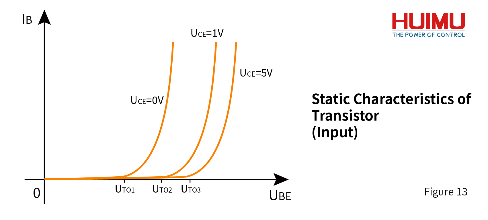
The input characteristic of the transistor is similar to the forward input characteristic of the power diode, as shown in Figure 13.
When UCE is fixed value and UBE>UTO, the base current IB increases with the increase of UBE.
When UCE increases, UTO increases and the input characteristics curve moves to the right. This is because with the increase of UCE, part of the carriers that should be injected into the base region from the emitter region pass through the base region and are directly injected to the collector region, so the carrier concentration in the base region is too low to open the emitter junction (that is, the diffusion current of the emitter junction is less than or equal to the drift current). Therefore, it is necessary to increase UBE to make more carriers be injected into the base region from the emitter region (that is, the threshold voltage increases), and the input characteristic curve also moves to the right. When UCE increases to a certain extent, most of the carriers that can be injected into the base region from the emitter region are collected to the collector region, so even if UCE continues to increase, the input characteristics of the transistor can hardly be changed.
2- Output Characteristics
Before introducing the output characteristics of transistor, it is necessary to introduce the concept of DC load line. The DC load line is the volt-ampere characteristic curve of collector load RC (output terminal resistance) when the transistor is working in static state, IC = (EC - UCE) / RC. When the transistor enters the off state, it is equivalent to the collector circuit entering the off state. At this time, UCE=0, the voltage on RC is equal to the power supply voltage EC. When the transistor enters the on state, ICM is the possible maximum value of the output current IC, that is, the maximum current flowing through RC. Mark these two points in a rectangular coordinate system with IC as the Y axis and UCE as the X axis, and draw a line segment, that is, the DC load line. The intersection of the DC load line with the Y-axis is called the saturation point, and the intersection with the X-axis is called the cut-off point. The slope of the DC load line is the resistance value of RC.
The intersection of the DC load line and the output characteristics curve of the transistor is called the quiescent operation point, or Q point. When the transistor works at the static operating point, no matter how the AC signal in the input signal changes, the transistor can be guaranteed to work in a stable amplification state (that is, the emitter junction is forward biased, and the collector junction is reverse biased), and no nonlinear distortion will occur. When selecting the Q point, try to stay away from the saturation region (to avoid saturation distortion) and cut-off region (to avoid cut-off distortion) of the transistor to obtain the best amplification effect.
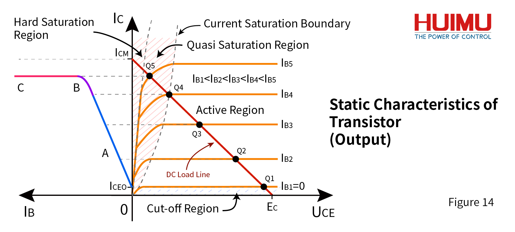
Since the transistor mainly outputs through the reverse current of the collector junction J1, its output characteristic curve is very similar to the static characteristic curve under the reverse bias of the power diode, as shown in Figure 14. Compared with power diodes, transistors have three working states. In order to understand the relationship between the output current IC and the input current IB intuitively, the X axis can be extended to the left, and the left part of the X axis can be regarded as the positive X half axis of IB. The Q points are projected to the second quadrant, which divide the characteristic curve of IC and IB into four sections: 0, A, B and C. These sections correspond to working region of the transistor.
Cut-off Region (Section 0): When UBE≤UTO or IB=0, the emitter junction is in the off state. At this time, even if the collector junction is reverse biased (UBC<0), the transistor is still in the off state (in fact, there is a very small penetration current ICEO). Similarly, if the collector junction is in the off state (IC=0), even if the emitter junction is forward biased (UBE>0), the transistor will not be turned on. Therefore, the cut-off condition of the transistor is, IC * IB = 0.
Active Region (Section A): When the emitter junction is forward biased and greater than the threshold voltage (UBE>UTO>0), IB>0, if the collector junction is reverse biased (UBC≤0), the transistor works in the active region (amplification region). At this time, the value of IC has nothing to do with UCE, but is only affected by IB, and there is a linear relationship between IB and IC, IC = β * IB.
Saturation Region (Section B and Section C): As the base current increases, the number of holes in the base region decreases, and the carriers injected into the base region from the emitter region also decreases, and the depletion layer of the base region widens. When the saturation boundary is reached, the amplification capability of the transistor begins to weaken (β' = ΔIC / ΔIB < β), IB and IC no longer have a linear relationship, and the transistor starts to enter the quasi-saturation state (shallow saturation state, Section B). When the number of holes in the base region drops to a critical value, the potential of the base region is the same as the potential of the collector region, that is, the collector junction J1 is in zero bias (UBC=0), and the base current completely loses the amplification effect (β' = ΔIC / ΔIB =0), and the transistor enters the fully saturated state (deep saturation state, Section C).
When the transistor is shallowly saturated, the base current IB is small and the conduction voltage drop is large, that is, the equivalent resistance of the transistor is large, so it is easy to exit the saturation state. When the transistor is deeply saturated, the base current IB is large and the conduction voltage drop is small, that is, the equivalent resistance of the transistor is small, and as IB increases, the saturation of the transistor will continue to deepen, so it is difficult to exit the saturation state. In actual operation, when IB(sat) = EC / (β * ICM), it can be considered that the transistor has entered the deep saturation state, which is the saturation state in the usual meaning. Sometimes in order to accelerate the transistor into the deep saturation state, a base current that is several times IB(sat) is applied. It should be noted that the working status of the transistor is also affected by the output resistance RC -- the smaller the output resistance RC, the larger the saturation current IC, and the larger the saturation voltage drop UCE, and the larger the saturation trigger current IB. As the output resistance RC decreases, the saturation current IC will approach ICM, making the transistor easily burned. If the output resistance RC is close to 0, even if the transistor is burned out, it cannot enter the saturation state. Therefore, a larger output resistance can make the transistor more likely to enter the saturation state.
3- Temperature
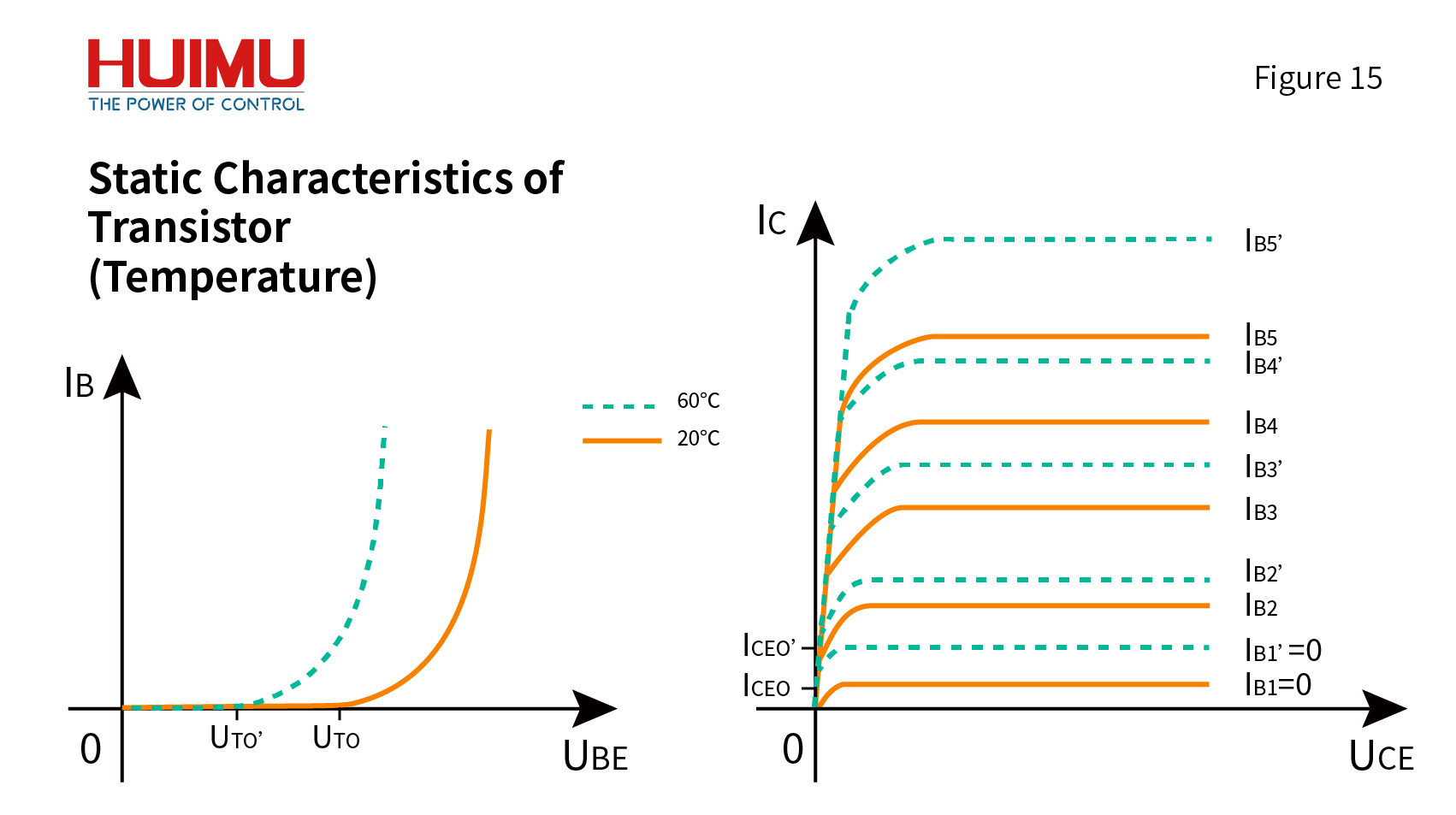
The increase in temperature will cause the intrinsic thermal excitation of the semiconductor, which will increase the carrier concentration inside the semiconductor and increase its conductivity. An increase in conductivity will cause an increase in leakage current, a decrease in threshold voltage, an increase in current gain and etc. Therefore, the input characteristic curve of the transistor will move to the right as the temperature rises, and the output characteristic curve of the transistor will move up as the temperature rises. The increase in temperature will also increase the possibility of the transistor thermal breakdown, so in actual use, sufficient heat dissipation conditions should be equipped to the transistor.
4- Safe Operating Area
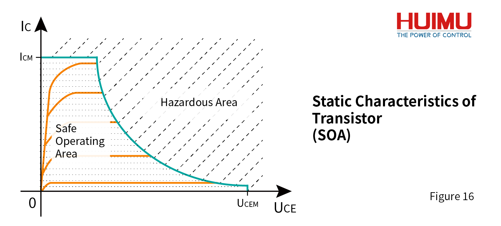
If the model of a transistor is known, its PCM parameters is also known. Through PCM=IC * UCE, PCM curve can be drawn. The ICM, UCEM, PCM curves can determine the safe operating area (SOA) of the transistor, in this area, the transistor can work stably without damage. The area outside the safe operating area is a hazardous area. In the hazardous area, the temperature of the transistor will increase significantly, making it more susceptible to thermal breakdown. Therefore, the transistor should be avoided to work in hazardous areas.
3.4.2 Dynamic Characteristics of Transistors
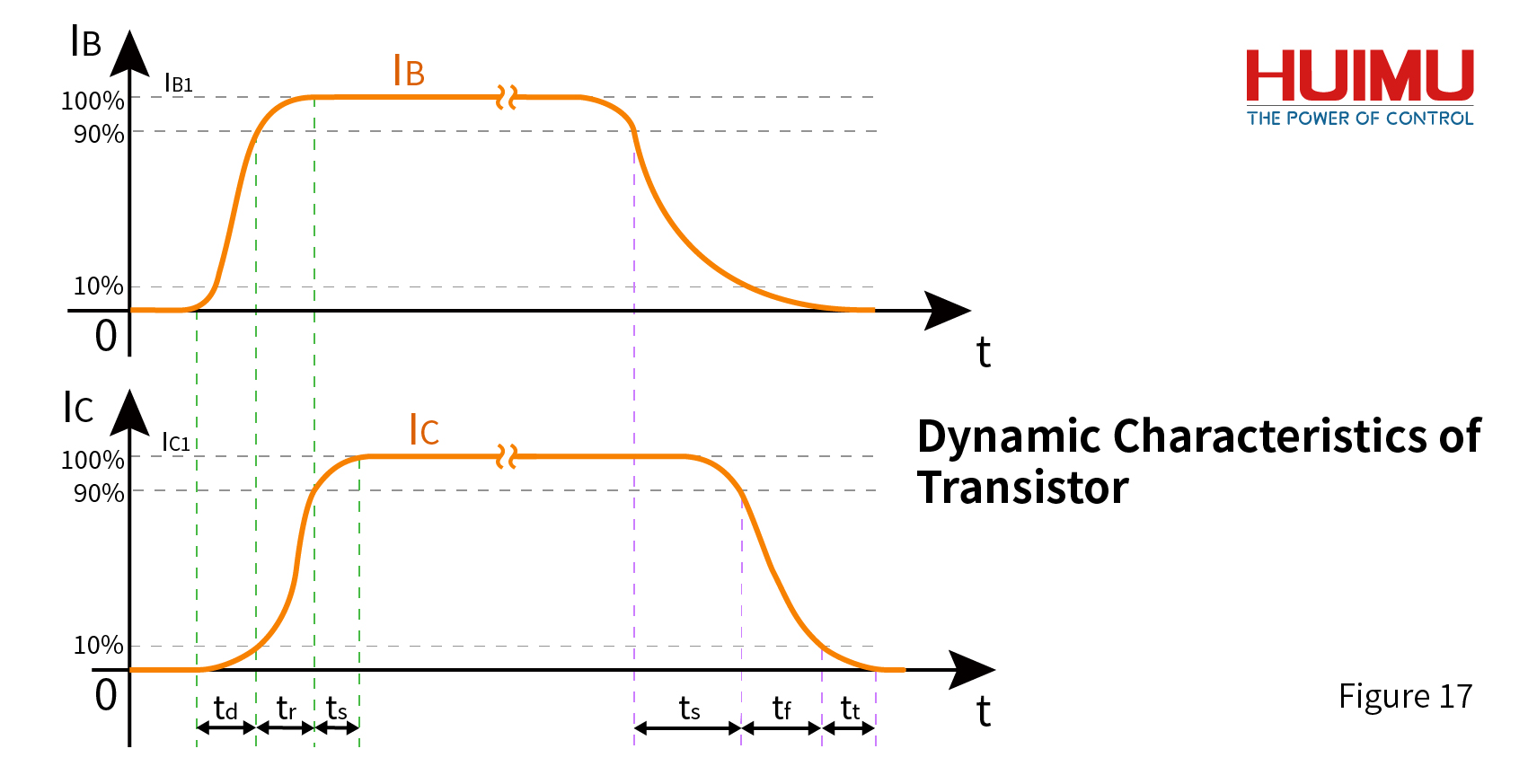
1- Turn-on process
When the turn-on condition (UBE> UTO) is met, the transistor will be turned on. The turn-on process of the transistor is divided into the delay time td, the rise time tr, and the diffusion time ts.
The delay time td is the time taken from 10% IB1 to 10% IC1. This time period is the time required to charge the barrier capacitor.
The rise time tr is the time taken for IC to go from 10% IC1 to 90% IC1. During this time period, IC rose sharply.
The diffusion time ts is the time taken for IC to go from 90% IC1 to 100% IC1. This time period is the time required to charge the diffusion capacitor.
The calculation formula of the turn-on time: ton=td + tr + ts
2- Turn-off process
When the cut-off condition (IB=0) is met, the transistor will be turned off. The turn-off process of the transistor is divided into the storage time ts, the fall time tf, and the tail time tt.
The storage time ts is the time taken from 90% IB1 to 90% IC1. This time period is the time required to remove the carriers stored in the base region during saturated conduction.
The fall time tf is the time taken for IC to fall from 90% IC1 to 10% IC1. During this time period, IC dropped sharply.
The tail time tt is the time taken for IC to fall from 10% IC1 to ICEO. This time period is the time required for the recombination of the remaining carriers.
The calculation formula of the turn-off time: toff = ts + tf + tt
