§2. What is the Structure of Solid State Relays

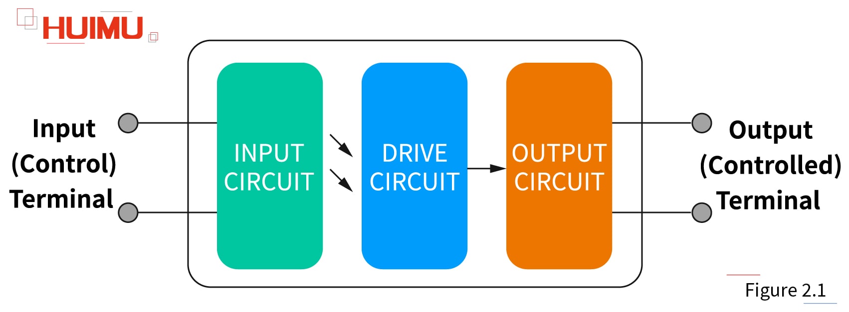
The solid-state relays are four-terminal active devices, two of the four terminals are input control terminals, and the other two terminals are output control terminals. Although the types and specifications of SSR switches are numerous, their structures are similar and consist mainly of three parts (as shown in Figure 2.1): Input Circuit (Control Circuit), Drive Circuit, and Output Circuit (Controlled Circuit).
Input Circuit:
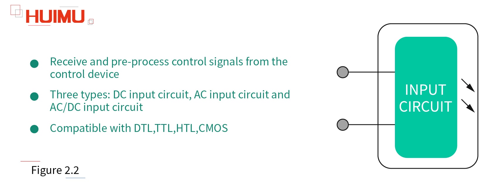
The Input Circuit of the solid state relay, also called control circuit, provides a loop for the input control signal, making the control signal as a trigger source for the solid state relay. According to different input voltage types, the input circuit can be divided into three types, DC input circuit, AC input circuit and AC/DC input circuit.

The DC input circuit can be further divided into Resistive Input Circuit and Constant Current Input Circuit.
1) The Resistive Input Circuit, whose input current increases linearly with increasing input voltage, and vice versa. If the control signal has a fixed control voltage, the resistor input circuit should be selected.
2) The Constant Current Input Circuit. When the input voltage of the constant current input circuit reaches a certain value, the current will no longer increase obviously as the voltage increases. This feature allows the use of a constant current input solid state relay over a fairly wide input voltage range. For example, when the voltage variation range of the control signal is kind of large (e.g., 3~32V), the DC solid state relay with constant current input circuit will be recommended to ensure that the DC solid-state relay can work reliably over the entire input voltage range.
Some of these input control circuits have positive and negative logic control, inverting and other functions, as well as the compatibility of logic circuits. Thus, solid state relays can be easily connected to TTL circuits (Transistor-Transistor Logic circuits), CMOS circuits (Complementary Metal Oxide Semiconductor circuits), DTL circuits (Diode-Transistor Logic circuits), and HTL circuits (High Threshold Logic circuits). At present, DTL has been gradually replaced by TTL, and HTL has been replaced by CMOS. And if the Pulse Width Modulated signal (PWM) is used as input signal, the ON/OFF switching frequency of the AC load supply should be set to less than 10Hz, or the output switching rate of the output circuit of the AC SSR cannot keep up with it.
Drive Circuit:
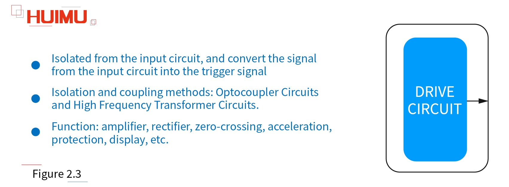
The driving circuit of solid state relay includes three parts: Isolation Coupling Circuit, Function Circuit and Trigger Circuit. However, according to the actual needs of solid-state relay, only one/two of these parts may be included.

1. Isolated Coupling Circuit:
The isolation and coupling methods for I/O circuits (Input / Output circuit) of solid-state relays currently use two ways, Optocoupler Circuits and High Frequency Transformer Circuits.
1) Optocoupler (also called photocoupler, optical coupler, opto-isolator, or optical isolator) is opaquely packaged with an infrared LED (Light-Emitting Diode) and an optical sensor to achieve isolated control between "control side" and "load side", because there is no electrical connection or physical connection between the " Light emitter " and the " Light sensor" except the beam. The types of "source-sensor" combinations normally include: "LED-Phototransistor" (Phototransistor Coupler), "LED-Triac" (Phototriac Coupler), and "LED-Photodiode array" (the stack of photodiodes is used to drive a pair of MOSFETs or an IGBT).
2) The high frequency transformer coupling circuit uses a high frequency transformer to convert the control signal at the input to the drive signal at the output. The detail process is, the input control signal produces a self-oscillating high frequency signal that will be transmitted through the transformer core to the transformer secondary, and after processing by the detection/rectification circuit and the logic circuit, the signal will eventually become the drive signal to drive the trigger circuit.
2. Functional Circuit:
The functional circuit may include various functional circuits, such as detection circuit, rectifier circuit, zero-crossing circuit, acceleration circuit, protection circuit, display circuit, etc.
3. Trigger Circuit:
The trigger circuit is used to provide a trigger signal to the output circuit.
Output Circuit:
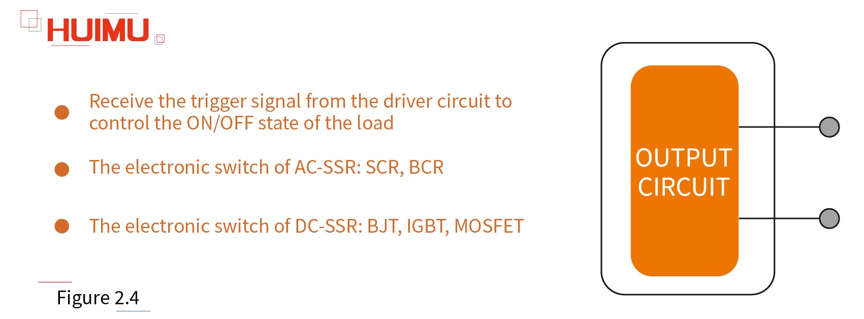
The output circuit of the solid-state relay is controlled by a trigger signal to enable on/off switching of the load power supplies.

The output circuit is mainly composed of an output component (chip) and an absorption loop (which acts as a transient suppressor), and sometimes includes a feedback circuit. Up to now, the output component of solid state relays mainly include: Bipolar Junction Transistor (Bipolar Transistor or BJT, which divided of two types, PNP and NPN), Thyristor (Silicon Controlled Rectifier or SCR), Triac (Bi-directional Triode, Bi-directional thyristor, Bi-directional Controlled Rectifier or BCR), Metal-Oxide-Semiconductor Field-Effect Transistor (MOSFET), Insulated Gate Bipolar Transistor(IGBT), Silicon-Carbide MOSFET (SIC MOSFET, a kind of wide bandgap transistor with the industrial grade highest operating junction temperature of 200°C, low power consumption and compact size), and so on.
The output circuit of the solid state relay can be divided into three types: DC output circuit, AC output circuit and AC/DC output circuit. The DC output circuit typically uses bipolar component (such as IGBT or MOSFET) as the output component, and the AC output circuit usually uses two Thyristors or one Triac as the output component.
